Thick copper circuit board with 12 OZ outer layer and solder-resist manufacturing method of thick copper circuit board

A technology of thick copper circuit board and manufacturing method, which is applied in the directions of printed circuit manufacturing, printed circuit, and printed circuit secondary processing, etc. Problems such as poor thickness uniformity can save costs and production time, improve reliability and quality, and avoid uneven ink.

Active Publication Date: 2014-11-12
KALEX MULTI LAYER CIRCUIT BOARD (ZHONGSHAN) CO LTD
View PDF4 Cites 0 Cited by
  • Summary
  • Abstract
  • Description
  • Claims
  • Application Information

AI Technical Summary

Problems solved by technology

[0004] (1) For the coating of solder resist (commonly known as green oil), according to the existing electrostatic spraying and printing method, the thickness uniformity of the green oil coating on the line with a bottom copper thickness of up to 12OZ is poor. The thickness is difficult to be guaranteed, and the uniformity of the green oil thickness on the wire surface cannot be guaranteed, which may easily cause oxidation or short circuit of exposed copper on the surface, affecting the electrical performance of the product and the safety of long-term use
[0005] (2) There are sharp corners on the top edge of the line, and the ink adhesion is poor
Because the outer 12OZ thick copper plate will produce a large side erosion effect during etching, the sharp corners of the top of the line will have poor adhesion, which will seriously affect the adhesion, thickness and reliability requirements of the line green oil
[0006] (3) Due to repeated etching of the outer 12OZ thick copper circuit, the side erosion of the circuit is more serious than that of ordinary copper, and there are likely to be gaps at the contact between the ink and the circuit. When the surface treatment such as sinking tin is easy to cause the circuit to be corroded due to the original battery effect, affecting the electrical performance and product reliability
[0007] (4) During the drilling process, due to the mismatch between resin drilling and thick copper drilling, it is easy to cause resin cracking at the edge of the hole
[0008] It can be seen that the existing production methods have potential safety hazards affecting the quality and reliability of solder mask production.

Method used


Image

  • Thick copper circuit board with 12 OZ outer layer and solder-resist manufacturing method of thick copper circuit board
  • Thick copper circuit board with 12 OZ outer layer and solder-resist manufacturing method of thick copper circuit board
  • Thick copper circuit board with 12 OZ outer layer and solder-resist manufacturing method of thick copper circuit board

Examples


Embodiment 1

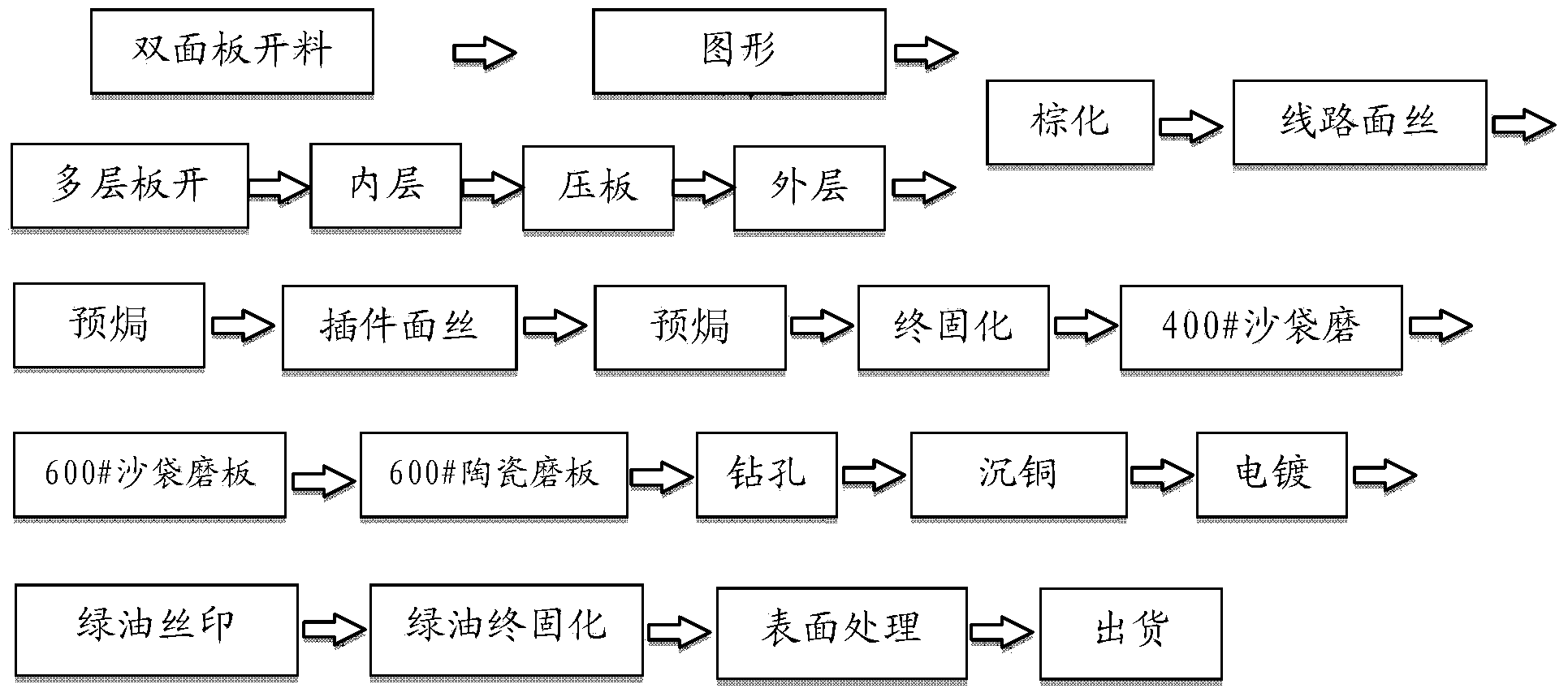
[0072] A kind of anti-soldering manufacturing method of outer layer 12OZ thick copper circuit board, comprises the following steps (flow chart sees figure 1 ):

[0073] (1) Browning of the outer circuit board; the weight percentage of sodium hypochlorite is 4.3%, the weight percentage of hydrogen peroxide is 4.8%, the temperature is 35°C, and the etching rate is 1.5 μm / cm 2 .

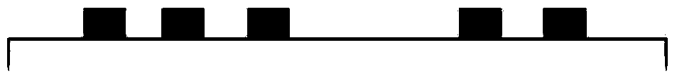
[0074] (2) Resin coating between 12OZ lines: use silk screen printing method to coat Shanrong special line resin ink between lines, let stand for 20min until the bubbles overflow, and then pre-bake and solidify; the technical parameters of the silk screen method are: : The angle of the squeegee of the screen printing machine is 25°, the thickness of the squeegee is 30mm, and the screen is slanted at 15° to print; Baking parameters: temperature is 120°C, time is 45min, curing parameters: temperature is 180°C, time is 60min;

[0075] (3) Grinding plate: 2 sandbag grinding plates and 1 ceramic grinding ...

Embodiment 2

[0095] The solder resist manufacturing method of the outer layer 12OZ thick copper circuit board described in the present embodiment, the steps are basically the same as in Embodiment 1, the difference is that:

[0096] (1) Browning of the outer circuit board: the weight percentage of sodium hypochlorite is 4%, the weight percentage of hydrogen peroxide is 4%, the temperature is 32°C, and the etching rate is 1.45 μm / cm 2 .

[0097] (2) Resin coating between lines: The technical parameters of the screen printing method are: the angle of the squeegee of the screen printing machine is 20°, the length of the squeegee is 25mm, and the screen is drawn at 13°; Method Pre-baking parameters of printed plug-in surface, line surface and plug-in surface: temperature is 110°C, time is 40min, curing parameters: temperature is 170°C, time is 50min;

[0098] (3) Grinding plate: use 1 sandbag grinding plate and 1 ceramic grinding plate, that is, use 400# sandbag grinding plate-600# ceramic gr...

Embodiment 3

[0109] The solder resist manufacturing method of the outer layer 12OZ thick copper circuit board described in the present embodiment, the steps are basically the same as in Embodiment 1, the difference is that:

[0110] (1) Browning of the outer circuit board: the weight percentage of sodium hypochlorite is 5%, the weight percentage of hydrogen peroxide is 6%, the temperature is 38°C, and the etching rate is 1.6 μm / cm 2 .

[0111] (2) Resin coating between lines: the technical parameters of the screen printing method are: the angle of the squeegee of the screen printing machine is 30°, the length of the squeegee is 35mm, and the screen is 17° inclined; In the same way, the pre-baking parameters of the Indy plug-in side, the circuit side and the plug-in side: the temperature is 130°C, the time is 50min, and the curing parameters: the temperature is 190°C, the time is 70min;

[0112] (3) Grinding plate: use sandbag grinding plate 3 times and ceramic grinding plate 2 times, that...


PUM


Abstract

The invention discloses an outer layer 12OZ thick-copper circuit board and a solder-mask manufacturing method of the outer layer 12OZ thick-copper circuit board. The method comprises the following steps of carrying out brown oxidation on outer layer circuits, carrying out resin coating among circuits, grinding a plate, drilling a hole and carrying out green oil silk screen. When resin coating among the circuits is carried out, resin ink is coated among the circuits by adopting a silk-screen method, standing is carried out for 10min to 30min for bubbles to be overflown, and pre-baking and solidification are carried out. The technical parameters of the silk-screen method are as follows: a squeegee angle of a screen printing machine is 20 degrees to 30 degrees, a scrapper is 25mm to 35mm, a silk screen is tensioned obliquely in 13 degrees to 17 degrees. When the plate is grinded, sandbag plate grinding is adopted for one to three times and ceramic plate grinding for one or twice. The hole is drilled by being divided into three sections, the proportion of all sections is 1 : 0.9 to 1.1 : 0.9 to 1.1. According to the solder-mask manufacturing method of the outer layer 12OZ thick-copper circuit board, solder-mask performance of outer layer circuits is improved by adopting an increasing method, the phenomena that oil ink is uneven, copper is exposed due to oil leakage and partial circuits corrode after surface treatment, and the outer layer 12OZ thick-copper circuit board is made to be good in appearance, electrical performance and reliability.

Description

technical field [0001] The invention relates to a method for manufacturing a circuit board with anti-soldering, in particular to a circuit board with an outer layer of 12OZ thick copper and a method for manufacturing the same. Background technique [0002] The outer 12OZ thick copper circuit board is used as an automotive electronic component, especially in high-power and high-voltage parts such as engine power supply parts and automotive central electrical power supply parts. It requires circuit boards to have characteristics such as heat aging resistance and high and low temperature cycle resistance. [0003] However, the current green oil anti-soldering technology of the outer layer 12OZ thick copper plate has the following technical difficulties and hidden dangers in reliability: [0004] (1) For the coating of solder resist (commonly known as green oil), according to the existing electrostatic spraying and printing method, the thickness uniformity of the green oil coati...

Claims


Application Information

Patent Timeline
Patent Type & Authority Applications(China)
IPC IPC(8): H05K1/00H05K3/28H05K3/00
Inventor 谭健文
Owner KALEX MULTI LAYER CIRCUIT BOARD (ZHONGSHAN) CO LTD
Why Eureka
Try Eureka