Method for preparing Bi2Se3 thin film by virtue of magnetron sputtering process

A magnetron sputtering and thin film technology, applied in the preparation of Bi2Se3 thin films and thin film materials, can solve the problems of slow epitaxial growth rate, expensive preparation equipment, large energy consumption, etc. The effect of low production cost

Active Publication Date: 2014-11-19
中天苏武(苏州)新材料科技有限公司
View PDF6 Cites 13 Cited by
  • Summary
  • Abstract
  • Description
  • Claims
  • Application Information

AI Technical Summary

Problems solved by technology

However, the vacuum conditions required for its preparation are extremely high (to reach 10 -8 Pa), the epitaxial growth rate is extremely slow (about 1um/hour), and the pre

Method used


Image

  • Method for preparing Bi2Se3 thin film by virtue of magnetron sputtering process
  • Method for preparing Bi2Se3 thin film by virtue of magnetron sputtering process
  • Method for preparing Bi2Se3 thin film by virtue of magnetron sputtering process

Examples


Embodiment 1

[0022] Preparation of Bi by a magnetron sputtering method 2 Se 3 The method of thin film, its step is:

[0023] a. Clean the substrate: ultrasonically clean the silicon substrate in acetone, ethanol, and deionized water for 10 minutes;

[0024] b. Sputtering preparation: dry the silicon substrate with hot nitrogen and place it on the substrate of the magnetron sputtering equipment, and install Bi with a purity of 99.99% on the sputtering target of the magnetron sputtering equipment 2 Se 3 For the target material, adjust the distance between the sputtering target and the silicon substrate to be 5 cm;

[0025] c. Sputtering Bi 2 Se 3 Thin films: evacuate the sputtering chamber to a pressure of 1.9×10 -4 Pa, and then pass in argon gas with a purity of 99.995%, so that the pressure of the sputtering chamber is 0.5Pa, adjust the substrate temperature to 360°C, and perform sputtering power to 6W / cm 2 , Sputtering deposition with a time of 60 seconds;

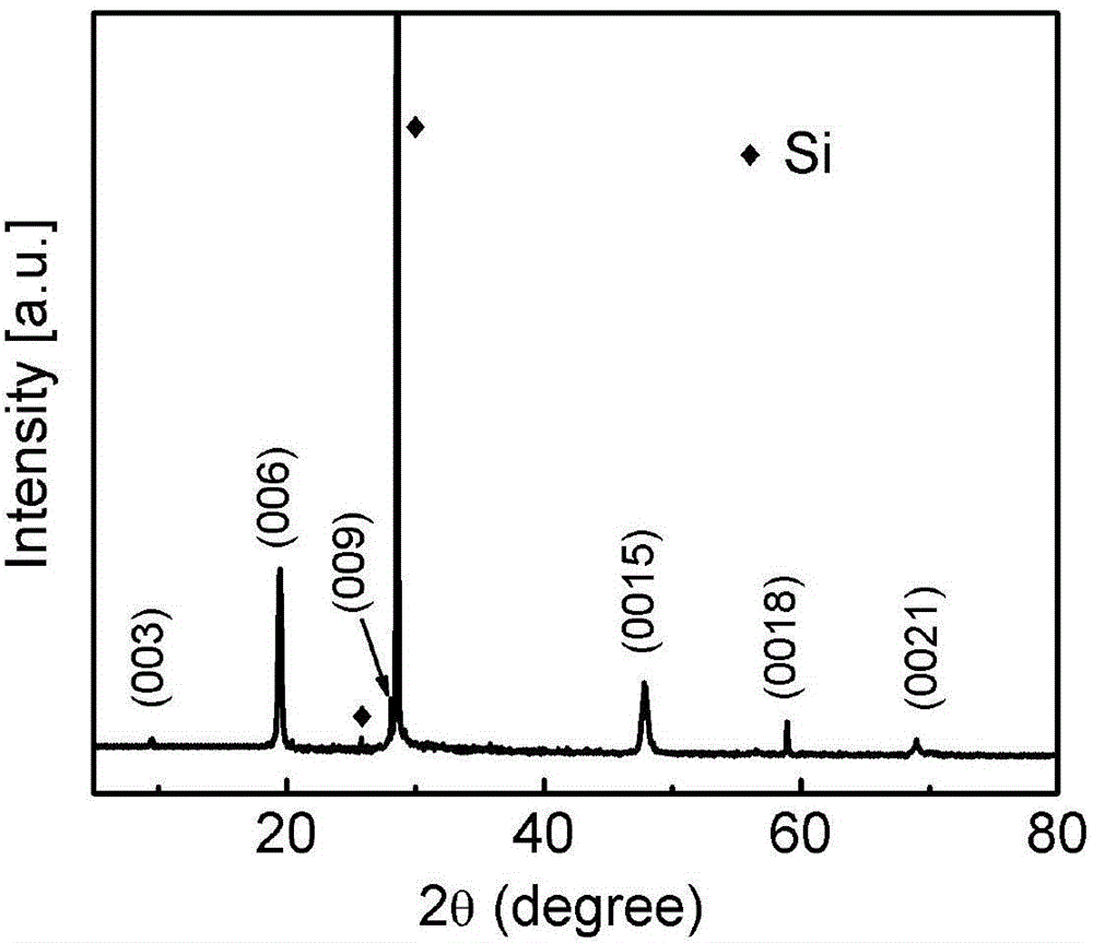
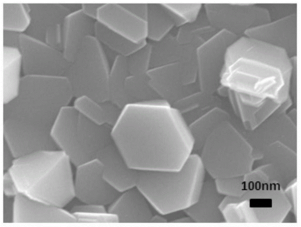
[0026] d. Post-anneali...

Embodiment 2

[0031] Preparation of Bi by a magnetron sputtering method 2 Se 3 The method of thin film, its step is:

[0032] a. Clean the substrate: ultrasonically clean the silicon substrate in acetone, ethanol, and deionized water for 15 minutes;

[0033] b. Sputtering preparation: dry the silicon substrate with hot nitrogen and place it on the substrate of the magnetron sputtering equipment, and install Bi with a purity of 99.99% on the sputtering target of the magnetron sputtering equipment 2 Se 3 Target material, adjust the distance from the sputtering target to the silicon substrate to be 6 cm;

[0034] c. Sputtering Bi 2 Se 3 Thin film: evacuate the sputtering chamber to a pressure of 1.8×10 -4 Pa, and then inject argon gas with a purity of 99.995%, so that the pressure of the sputtering chamber is 0.4Pa, adjust the substrate temperature to 360°C, and perform sputtering power to 4W / cm 2 , sputter deposition for 300 seconds;

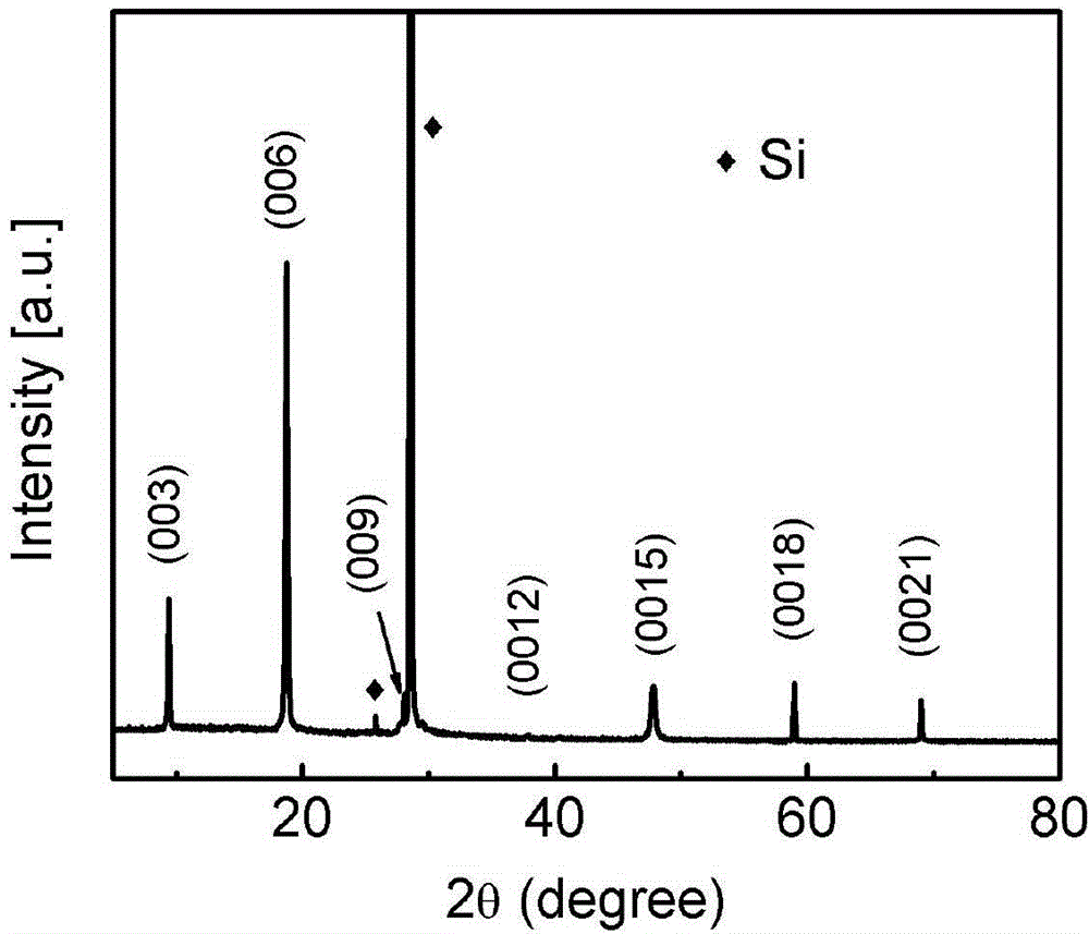
[0035] d. Post-annealing treatment: the deposition ...

Embodiment 3

[0040] Preparation of Bi by a magnetron sputtering method 2 Se 3 The method of thin film, its step is:

[0041] a. Clean the substrate: ultrasonically clean the silicon substrate in acetone, ethanol, and deionized water for 20 minutes;

[0042] b. Sputtering preparation: dry the silicon substrate with hot nitrogen and place it on the substrate of the magnetron sputtering equipment, and install Bi with a purity of 99.99% on the sputtering target of the magnetron sputtering equipment 2 Se 3 Target material, adjust the distance from the sputtering target to the silicon substrate to be 7 cm;

[0043] c. Sputtering Bi 2 Se 3 Thin films: evacuate the sputtering chamber to a pressure of 1.6×10 -4 Pa, and then feed argon gas with a purity of 99.995%, so that the pressure of the sputtering chamber is 0.6Pa, adjust the substrate temperature to 360°C, and perform sputtering power to 5W / cm 2 , Sputtering deposition with a time of 600 seconds;

[0044] d. Post-annealing treatment: ...


PUM


Abstract

The invention discloses a method for preparing a Bi2Se3 thin film by virtue of a magnetron sputtering process. The method mainly comprises the following steps: a, substrate cleaning; b, sputtering preparation: drying silicon substrates, putting the silicon substrates on an underlayer, and assembling a Bi2Se3 target material of which the purity is 99.99% on a sputtering target; c, Bi2Se3 thin film sputtering: performing vacuum pumping on a sputtering chamber until the air pressure is less than 2*10<-4>Pa, then introducing 99.995% of argon to ensure that the air pressure of the sputtering chamber is 0.4-0.6Pa and the temperature of the underlayer is 360 DEG C, and performing sputtering deposition for 60-600 seconds at a power of 4-6W/cm<2>; d, post-annealing treatment: sealing deposited silicon substrates and selenium particles into a vacuum quartz tube of which the air pressure is less than 1*10<-2>Pa, putting into a tubular furnace, and performing post-annealing treatment for 2-3 hours at 250-300 DEG C under an argon protective atmosphere to obtain the Bi2Se3 thin film. The method disclosed by the invention is low in vacuum condition requirement, short in preparation time and low in cost.

Description

technical field [0001] The invention belongs to the technical field of film material preparation, in particular to Bi 2 Se 3 The technical field of thin film preparation. Background technique [0002] Bi 2 Se 3 Belonging to the bismuth tellurite compound, it has attracted people's attention for its excellent thermoelectric properties and far-infrared properties, and has been widely used in the semiconductor refrigeration industry as a thermoelectric material. Recently, it has been found that single crystal Bi 2 Se 3 It is a topological insulator material, which may play a big role in the field of quantum computers and spintronics devices to realize the transmission of signals with almost no energy dissipation. In recent years, with the continuous improvement of device performance requirements, device design is developing in the direction of miniaturization, novel structure, low-dimensional space, and energy quantization. Therefore, the miniaturization and low-dimensio...

Claims


Application Information

Patent Timeline
IPC IPC(8): C23C14/35C23C14/58C23C14/06
Inventor 羊新胜魏占涛张敏赵勇闫勇
Owner 中天苏武(苏州)新材料科技有限公司
Why Eureka
Try Eureka