Technology for manufacturing fast recovery diode
A recovery diode and manufacturing process technology, applied in semiconductor/solid-state device manufacturing, electrical components, circuits, etc., can solve problems such as difficult implementation, far-reaching mature technology, and lack of nuclear radiation in microelectronics factories, so as to achieve a good recovery diode device Effect
- Summary
- Abstract
- Description
- Claims
- Application Information
AI Technical Summary
Problems solved by technology
Method used
Image
Examples
Embodiment 1
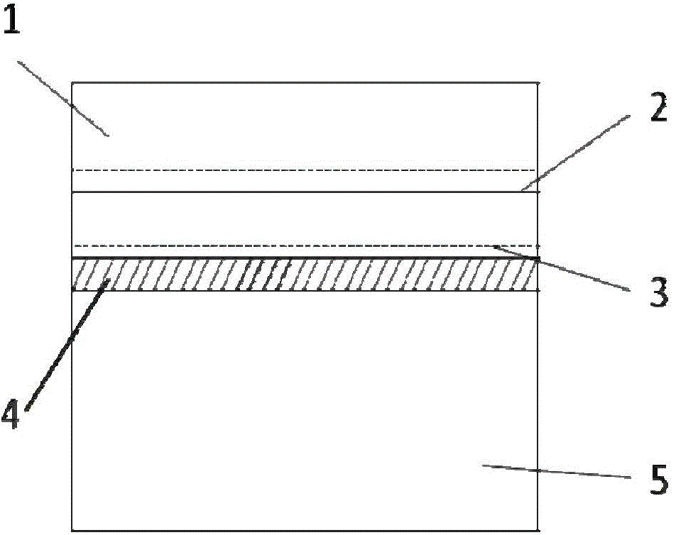
[0043] Take an N-doped silicon substrate wafer; carry out ion implantation, first ion implantation of protons (hydrogen ions), introduce defect regions into the depth of the substrate sheet about 1.2-1.5 μm, then ion implantation of boron ions, in the substrate Introduce P-type doping at about 0-0.5 μm on the shallower surface of the bottom; perform laser annealing of the implanted boron element, and use a 532nm laser beam for laser annealing. While annealing the area within 1 μm depth on the wafer surface, it does not touch the deeper proton implantation damage area, so the basic structure of the PN junction is formed after laser annealing, and a defect damage area is maintained in the body; Platinum treatment, the platinum diffusion temperature is 750°C, 15-20 minutes under the nitrogen atmosphere, due to the effect of diffusion and gettering in the defect area, the introduced platinum atoms will gather more in the depth range of 1.2-1.5μm; Electrode fabrication, passivation...
Embodiment 2
[0046]Take a P-doped silicon substrate wafer; first, high-energy ions are implanted with boron ions, and defect regions are introduced into the depth of the substrate about 1.0-1.2 μm, and then ions are implanted with phosphorous ions, about 0 on the shallower surface of the substrate. Introduce N-type doping at -0.3μm; perform laser annealing of the injected phosphorus element, laser annealing is carried out with a 532nm laser beam, because the penetration depth of the laser at this wavelength into the silicon wafer is limited, combined with the action energy and action time Therefore, while annealing the area within 1 μm depth on the wafer surface, it does not touch the deeper boron ion implantation damage area, so the N+P-junction basic structure is formed after laser annealing, and a defect is maintained in the body Damaged area: For the treatment of platinum expansion on the substrate, the platinum diffusion temperature is 750°C, and it is under nitrogen atmosphere for 15-...
Embodiment 3
[0049] Take an N-doped silicon substrate wafer; perform ion implantation of boron ions, introduce P-type doping at about 0-0.3 μm on the shallower surface of the substrate; perform platinum metal sputtering on the surface of the silicon wafer to form about 5 -10nm platinum metal layer; laser annealing, laser annealing is carried out with a 532nm green laser to activate the boron ions on the shallower surface; at the same time, when the laser transmits energy to the metal platinum on the surface of the substrate, it will drive the boron ions on the surface Platinum moves deep into the silicon wafer, and on the other side, due to the limited depth of laser penetration into the silicon wafer, after platinum atoms move to a certain depth in the silicon wafer, they will slowly stop their movement because they cannot continue to receive the energy delivered by the laser. And stay at a specific depth; after that, process steps such as electrode fabrication, passivation, lead packaging...
PUM
 Abstract
Description
Claims
Application Information
