Cu2ZnSnS4 schottky diode structure and preparation method thereof

A technology of Schottky diodes and top electrodes, which is applied in semiconductor/solid-state device manufacturing, semiconductor devices, electrical components, etc., and can solve problems such as application limitations and device impact.

Inactive Publication Date: 2014-11-19
EAST CHINA NORMAL UNIVERSITY
View PDF4 Cites 0 Cited by
  • Summary
  • Abstract
  • Description
  • Claims
  • Application Information

AI Technical Summary

Problems solved by technology

[0003] At present, the conventional Schottky diode, its ohmic contact electrode is arranged on the back of the substrate, and the semiconductor thin film layer and the Schottky contact electrode

Method used


Image

  • Cu2ZnSnS4 schottky diode structure and preparation method thereof
  • Cu2ZnSnS4 schottky diode structure and preparation method thereof
  • Cu2ZnSnS4 schottky diode structure and preparation method thereof

Examples


Embodiment 1

[0029] Example 1: Cu 2 ZnSnS 4 Fabrication of Schottky Diode Structures

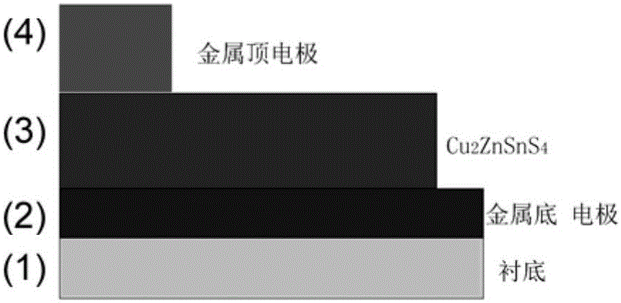
[0030] (1) Cleaning the glass substrate 1, using acetone, ethanol and deionized water to perform ultrasonic cleaning for 20 minutes in sequence, and after the cleaning is completed, the glass substrate 1 is placed in deionized water for preservation for later use. The glass substrate 1 was blown dry with a nitrogen gun before use. The substrate may also be a silicon wafer substrate or a stainless steel flexible substrate or other suitable substrate.

[0031] (2) A metal bottom electrode molybdenum is deposited on the glass substrate 1 using a magnetron sputtering process to form a metal bottom electrode layer 2 . The deposition process of metal molybdenum is as follows: sputtering with a radio frequency power source, the sputtering power is 80W, and the argon gas pressure is 1.2Pa during sputtering. The metal bottom electrode molybdenum is deposited to a thickness of about 1 micron.

[0032] (3) Pre...


PUM

PropertyMeasurementUnit
Thicknessaaaaaaaaaa

Abstract

The invention discloses a novel Cu2ZnSnS4 schottky diode structure and a preparation method thereof. The Cu2ZnSnS4 schottky diode structure comprises a substrate, a bottom metal electrode layer, a Cu2ZnSnS4 thin layer and a top metal electrode layer, wherein the bottom metal electrode layer, the Cu2ZnSnS4 thin layer and the top metal electrode layer are deposited on the substrate in sequence from bottom to top. According to the Cu2ZnSnS4 schottky diode provided by the invention, large series resistance in the device structure can be avoided, so that the ideal factor of the schottky diode can be optimized, and further, the cut-off frequency of the device is favorably improved, as a result, the structure is applicable to high frequency circuits; the schottky diode structure has the advantages of abundant raw material sources, low price, strong radiation resistance and antidamping capability, good stability, relatively diversified deposition methods and high selectivity in substrates, so that the device is flexible in structural design and the preparation technology is simple, as a result, the diode structure has a wide application prospect.

Description

technical field [0001] The invention relates to the technical field of semiconductor devices, in particular to a new type of Cu 2 ZnSnS 4 Schottky diode structure and preparation method thereof. Background technique [0002] Cu 2 ZnSnS 4 As a new type of semiconductor thin film material, thin film has received extensive attention. Cu 2 ZnSnS 4 The thin film is a direct bandgap semiconductor material with a forbidden band width of about 1.5eV and a high absorption coefficient (greater than 10 4 cm -1 ), the elements contained are relatively abundant in the crust, and the material stability is good. Based on the above advantages, the material has been widely used in the photovoltaic field. As a semiconductor material, Cu 2 ZnSnS 4 The thin film can also be used in metal-semiconductor-metal (MSM) devices to form Schottky diodes, which can be widely used in microwave mixing, detection, and high-speed switching. [0003] In the current conventional Schottky diode, the...

Claims


Application Information

Patent Timeline
IPC IPC(8): H01L29/872H01L29/12H01L21/329
CPCH01L29/872H01L29/417H01L29/66969
Inventor 何俊张俊孙琳杨平雄褚君浩
Owner EAST CHINA NORMAL UNIVERSITY
Why Eureka
Try Eureka