Inverted type organic electroluminescence structure

An inverted, electroluminescent technology, used in organic semiconductor devices, circuits, electrical components, etc., can solve the problems of difficult electron injection and high device driving voltage, achieve good conductivity and flexibility, and reduce the hole injection barrier. Effect

Inactive Publication Date: 2014-12-10
EVERDISPLAY OPTRONICS (SHANGHAI) CO LTD
View PDF9 Cites 20 Cited by
  • Summary
  • Abstract
  • Description
  • Claims
  • Application Information

AI Technical Summary

Problems solved by technology

[0004] like figure 1 As shown, the current inverted OLED structure uses the common ITO as the cathode. Due to the high work function of ITO, in order to efficiently inject electrons from ITO directly to the organic layer, a suitable EIL is needed, and this EIL material is very rare. With a suitable EIL material, the potential barrier for electron injection from the cathode will be relatively high, resulting in difficulty in electron injection and high device driving voltage

Method used


Image

  • Inverted type organic electroluminescence structure
  • Inverted type organic electroluminescence structure
  • Inverted type organic electroluminescence structure

Examples


Embodiment 1

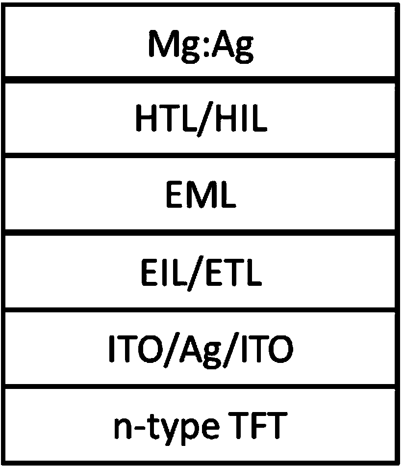
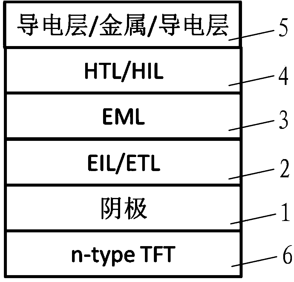
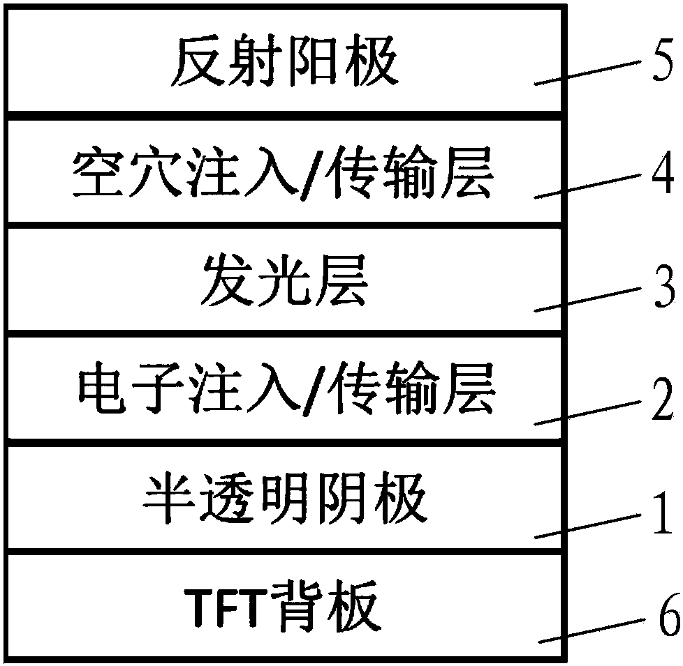
[0047] refer to image 3 , for the figure 2 On the basis of the structural schematic diagram of Embodiment 1, such as image 3 As shown, the first form of the inverted organic electroluminescence structure of the present invention is a bottom emission structure, including: a substrate 6 and a cathode layer 1 arranged on the substrate 6 from bottom to top, an electron injection transport layer 2, and a light emitting layer 3 , a hole injection transport layer 4 and an anode layer 5 . Wherein, the cathode layer 1 is a translucent, 25nm-thick Mg:Ag alloy, and the ratio of Mg:Ag is 1:9, 5:5 or 7:3, so that the transmittance of the cathode layer 1 is controlled at 21%; And anode layer 5 is ITO, Ag double-layer structure (without the second conductive layer), and promptly the first conductive layer is the thick ITO of 15nm, and its transmittance is greater than 85%, because the metal layer is the thick Ag of 150nm, with this, The reflectivity of the anode layer 5 is controlled a...

Embodiment 2

[0050] refer to Figure 6 ,exist figure 2 On the basis of the structural schematic diagram of embodiment two, as Figure 6 As shown, the second form of the inverted organic electroluminescence structure of the present invention: top emission structure,

[0051] 1) The device structure of the top emission structure is:

[0052] Substrate / Ag / Al / Alq3 / Bebq2: Ir(MDQ)2(acac) / NPB / HAT-CN / Ag / ITO.

[0053] 2) Preparation of cathode layer 1

[0054] Under the condition that the pressure of the vacuum chamber is 10-4Pa, a layer of metallic silver is first coated on the substrate 6, and then annealed at a high temperature of 400°C, and the self-aggregation of silver is used to form silver nanoparticles, and the height of the nanoparticles is 30- 50nm, and then coated with a layer of metal aluminum with a thickness of 150nm, at this time, the cathode has a high reflectivity.

[0055] 3) Preparation of organic light-emitting layer

[0056] Keeping the pressure of the vacuum chamber co...

Embodiment 3

[0060] refer to Figure 7 ,exist figure 2 On the basis of the structural schematic diagram of embodiment three, as Figure 7 As shown, the third form of the inverted organic electroluminescent structure of the present invention: a double-sided light emitting structure,

[0061] 1) The device structure of the double-sided light emitting structure is:

[0062] Substrate / Al / Alq3 / Bebq2: Ir(MDQ)2(acac) / NPB / CuPc / ITO.

[0063] 2) Preparation of cathode structure

[0064] Under the condition that the pressure of the vacuum chamber is 10-4Pa, a layer of metal aluminum with a thickness of 15nm is plated on the substrate 6, and the cathode has a high transmittance because the thickness is very thin.

[0065] 3) Preparation of organic light-emitting layer

[0066] Keeping the pressure of the vacuum chamber constant, the electron injection transport layer 2, the light emitting layer 3, and the hole injection transport layer 4 were successively evaporated. In this embodiment, the elec...


PUM


Abstract

The invention provides an inverted type organic electroluminescence structure. The inverted type organic electroluminescence structure comprises a substrate, and a cathode layer, an electron injection layer, an electron transport layer, a luminous layer, a hole injection layer, a hole transport layer and an anode layer, which are sequentially arranged on the substrate from bottom to top, wherein the anode layer comprises a first conducting layer, a metal layer and a second conducting layer, and the cathode layer contains chemical compositions of magnesium, aluminum, silver, ytterbium and samarium and alloy of the above compositions, or the magnesium, the aluminum, the silver, the ytterbium and the samarium mixed with zinc oxide. The inverted type organic electroluminescence structure reduces the electron injection potential barrier, and improves hole injection capacity.

Description

technical field [0001] The invention relates to an organic electroluminescent structure, in particular to an inverted organic electroluminescent structure. Background technique [0002] Inverted Organic Light Emitting Diode (Inverted Organic Light Emitting Diode) is the opposite of the general OLED device structure: the cathode is made on the substrate first, and then the anode conductive film is made after evaporating an organic film on the cathode. The advantage of IOLED is that it is especially suitable for combining with n-channel oxide (IGZO) thin film transistors, and the carrier mobility of IGZO is 20 to 30 times that of amorphous silicon, so that the charge and discharge of TFT to the pixel electrode can be greatly improved. Speed, improve pixel response speed, achieve faster refresh rate, and faster response also greatly improves pixel line scan rate, more intuitively, its resolution can reach full HD (full HD) or even ultra high definition ( Ultra Definition, reso...

Claims


Application Information

Patent Timeline
Patent Type & Authority Applications(China)
IPC IPC(8): H01L51/52H01L51/54
CPCH10K50/81H10K50/82H10K2102/00H10K2102/101H10K2102/321H10K71/00
Inventor 牟鑫鲁佳浩寇浩
Owner EVERDISPLAY OPTRONICS (SHANGHAI) CO LTD
Why Eureka
Try Eureka