A beam-membrane structure high-voltage electrostatic field sensor chip based on the pressure-sensitive principle

A high-voltage electrostatic field and sensor chip technology, applied in electrostatic field measurement and other directions, can solve problems such as low frequency or low electrostatic field sensitivity, inability to achieve mass production, sensor supply, etc., to improve measurement sensitivity and increase the stress concentration in sensitive areas. effect, single low cost effect

Inactive Publication Date: 2016-08-24
XI AN JIAOTONG UNIV
View PDF6 Cites 0 Cited by
  • Summary
  • Abstract
  • Description
  • Claims
  • Application Information

AI Technical Summary

Problems solved by technology

However, in the electrostatic field, the electric field cannot provide continuous energy to the sensor, and the charge on the high-voltage conductor cannot continue to maintain macroscopic motion. This has become a difficult point in the measurement of the electrostatic field, making the current electric field sensor less sensitive to low-frequency or electrostatic fields.
At the same time, the current sensors that can be used to measure high-voltage electrostatic fields have disadvantages such as complex structure, large volume, and high cost, and cannot be mass-produced
During the operation of the power system or electrical laboratory, a large number of non-contact indirect measuring instruments are required to monitor the accident-prone points of the high-voltage busbar on-line to ensure the safety of operators and electronic equipment. Therefore, the existing electric field Sensors cannot meet this requirement

Method used


Image

  • A beam-membrane structure high-voltage electrostatic field sensor chip based on the pressure-sensitive principle
  • A beam-membrane structure high-voltage electrostatic field sensor chip based on the pressure-sensitive principle
  • A beam-membrane structure high-voltage electrostatic field sensor chip based on the pressure-sensitive principle

Examples


Embodiment Construction

[0021] The present invention will be described in detail below in conjunction with the accompanying drawings.

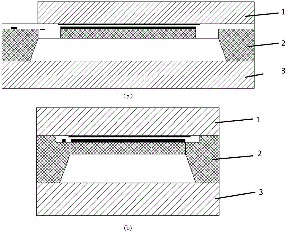
[0022] refer to figure 1 , a beam film structure high-voltage electrostatic field sensor chip based on the principle of pressure sensitivity, comprising a base 3, a silicon structure layer 2 is arranged on the base 3, an upper pole plate 1 is arranged on the silicon structure layer 2; the upper surface of the base 3 The lower surface of the silicon structure layer 2 is connected by anodic bonding, and the upper surface of the silicon structural layer 2 is connected with the lower surface of the upper plate 1 by anodic bonding.

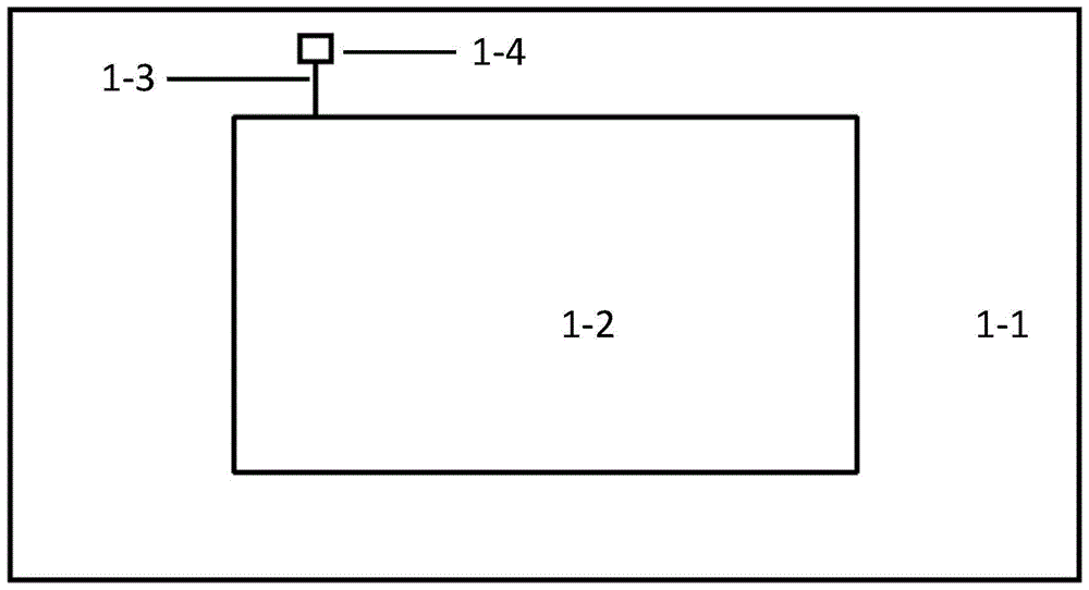
[0023] refer to figure 2 , the upper plate 1 is an electrode formed by depositing metal on the glass plate 1-1, and a rectangular fixed metal film electrode 1-2 is arranged in the middle area of ​​the lower surface of the glass plate 1-1, and the fixed metal film electrode 1-2 is A first electrode connection pad 1-4 is arranged beside the ...


PUM


Abstract

A beam-membrane structure high-voltage electrostatic field sensor chip based on the principle of pressure sensitivity, including a base, a silicon structure layer is arranged on the base, an upper pole plate is arranged on the silicon structure layer; the upper surface of the base and the lower surface of the silicon structure layer Connected by anodic bonding, the upper surface of the silicon structure layer and the lower surface of the upper plate are connected by anodic bonding, and the piezoresistive principle is used to measure the electrostatic field force, so as to obtain the electrostatic field strength; the method of beam-membrane combination makes the measurement sensitivity Greatly improved; the core film of the chip does not have a quality block, the thickness is small, and four beams are used to support the load-bearing film, which improves the structural rigidity, the sensor chip has a high frequency response, the connection is simple, the resistance bar and lead wire layout are easy to implement, the structure is stable, and the production The technology is mature, and the reliable packaging method can make the chip adapt to a variety of different environments; after the mass production of the chip, the single cost is very low, and the interface and installation are extremely simple, suitable for large-scale application in industrial sites.

Description

technical field [0001] The invention relates to the technical field of micro-electromechanical systems (MEMS) high-voltage electrostatic field sensors; in particular, it relates to a beam-membrane structure high-voltage electrostatic field sensor chip based on the principle of pressure sensitivity. Background technique [0002] High-voltage power capacitors are widely used in power systems and test stations. Because the charge stored in capacitors is in a static state, it is difficult to be sensed by general measurement methods, including electromagnetic induction, magnetic field measurement and other principles and methods. At present, it is used for high-voltage electrostatic induction The devices and products tested, including rotating vane type and vibrating capacitive electrostatic measuring devices, are technically and economically difficult to apply to high-voltage capacitors equipped in large quantities in the power sector due to their volume, large power consumption,...

Claims


Application Information

Patent Timeline
Patent Type & Authority Patents(China)
IPC IPC(8): G01R29/12
Inventor 赵玉龙白民宇耿英三翟小社
Owner XI AN JIAOTONG UNIV
Why Eureka
Try Eureka