Thin film transistor and preparation method thereof, array substrate and preparation method thereof and display device
A technology for thin film transistors and array substrates, applied in the display field, can solve the problems of low process yield, high fabrication cost of array substrates, long process time, etc., and achieve the effects of simplifying structure and manufacturing process, reducing impedance, and reducing parasitic capacitance
- Summary
- Abstract
- Description
- Claims
- Application Information
AI Technical Summary
Problems solved by technology
Method used
Image

Examples
Embodiment 1
[0080] This embodiment provides a thin film transistor and a corresponding manufacturing method of the thin film transistor.
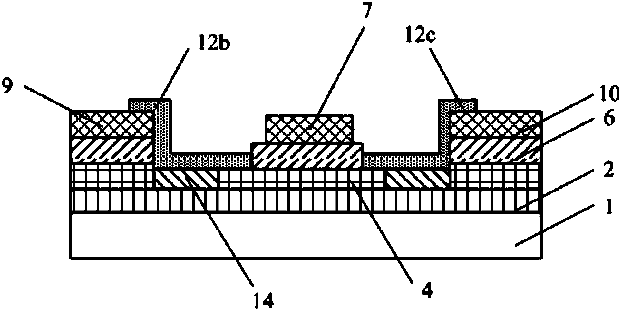
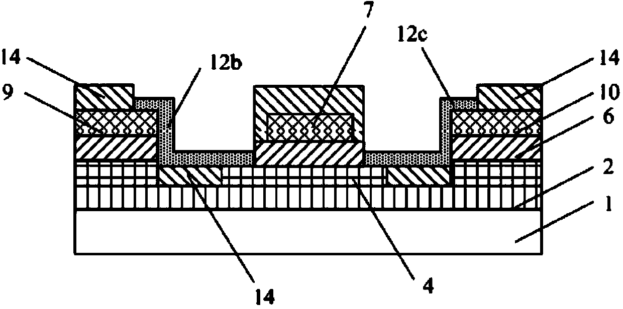
[0081] Such as Figure 2A and Figure 2B As shown, the thin film transistor includes a gate 7, a source 9, a drain 10, an active layer 4 and a gate insulating layer 6, wherein the gate insulating layer 6 is arranged above the active layer 4, and the gate 7, The source 9 and the drain 10 are arranged on the same layer above the gate insulating layer 6, the active layer 4 and the source 9 are connected through the first connection electrode 12b, and the active layer 4 and the drain 10 are connected through the second connection electrode 12c .
[0082] It should be understood here that, in the present invention, "same layer" refers to the layer structure formed by using the same film-forming process to form a film layer for forming a specific pattern, and then using the same mask to form a patterning process; according to the specific pattern differen...
Embodiment 2
[0120] This embodiment provides an array substrate and a corresponding manufacturing method of the array substrate. The array substrate includes the thin film transistor in Embodiment 1.
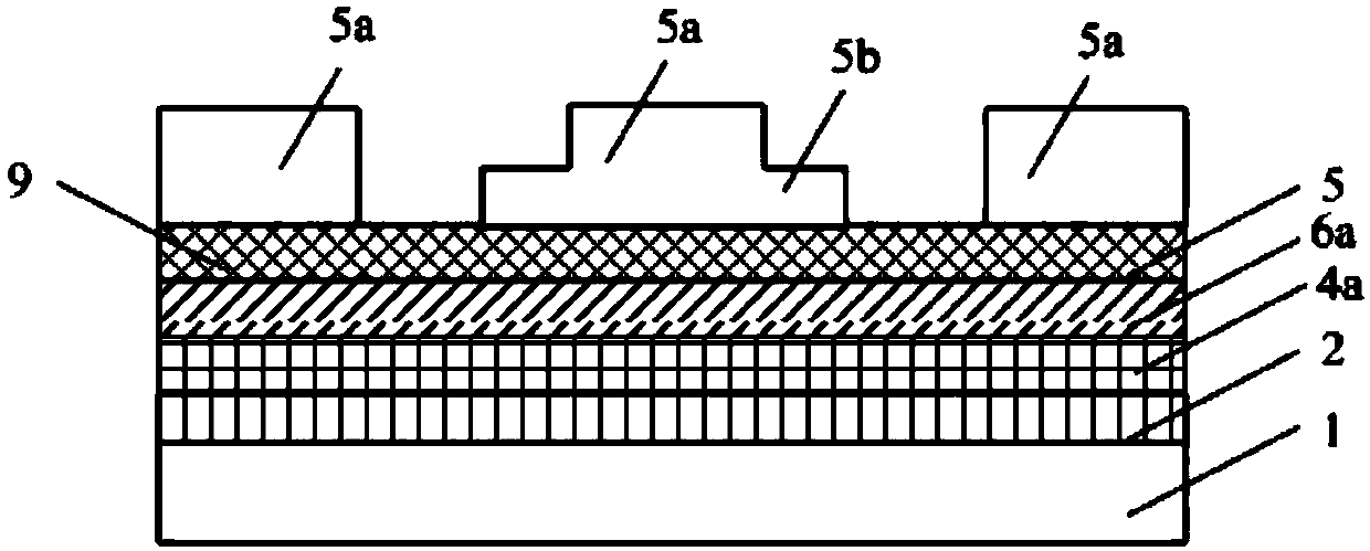
[0121] Such as Figure 4 Shown, in Example 1 Figure 3F Based on the thin film transistor shown, the array substrate of this embodiment further includes a passivation layer 11 and a pixel electrode 12. The passivation layer 11 is partially disposed above the drain 10 and formed on the side of the drain 10 close to the gate 7 The matching drain contact region 10b; the pixel electrode 12 is connected to the drain 10 by overlapping the matching drain contact region 10b and the drain contact region 4c (see Figure 5C , Figure 4 The mating source contact region 9c and source contact region 4b, the mating drain contact region 10b and the drain contact region 4c have been respectively covered by the first connection electrode 12b and the second connection electrode 12c, so they are not specific...
Embodiment 3
[0157] This embodiment provides a display device, which includes the array substrate in Embodiment 2.
[0158] According to the structure of the array substrate, the display device may be a liquid crystal display device or an organic electroluminescent diode display device. That is, the display device can be any product or component with a display function such as a liquid crystal panel, an electronic paper, an OLED panel, a mobile phone, a tablet computer, a television set, a monitor, a notebook computer, a digital photo frame, a navigator, and the like.
[0159] The display device is formed by using a low-temperature polysilicon array substrate, has good display effect, and has low manufacturing cost.
PUM
| Property | Measurement | Unit |
|---|---|---|
| Thickness | aaaaa | aaaaa |
| Thickness | aaaaa | aaaaa |
| Thickness | aaaaa | aaaaa |
Abstract
Description
Claims
Application Information
 - R&D
- Intellectual Property
- Life Sciences
- Materials
- Tech Scout
- Unparalleled Data Quality
- Higher Quality Content
- 60% Fewer Hallucinations
Browse by: Latest US Patents, China's latest patents, Technical Efficacy Thesaurus, Application Domain, Technology Topic, Popular Technical Reports.
© 2025 PatSnap. All rights reserved.Legal|Privacy policy|Modern Slavery Act Transparency Statement|Sitemap|About US| Contact US: help@patsnap.com