Blue-light LED (Light-Emitting Diode) epitaxial structure having asymmetrical barrier layer

An epitaxial structure, asymmetric technology, applied in electrical components, circuits, semiconductor devices, etc., can solve the problems of limiting the effective recombination probability of holes, large lattice mismatch, strong built-in electric field, etc., to suppress the phenomenon of electron overflow , the effect of improving internal quantum efficiency and improving crystal quality

Active Publication Date: 2014-12-31
NANTONG TONGFANG SEMICON +1
View PDF7 Cites 5 Cited by
  • Summary
  • Abstract
  • Description
  • Claims
  • Application Information

AI Technical Summary

Problems solved by technology

However, the active region 5 of the above-mentioned structure has the following disadvantages: first, due to the large lattice mismatch between the well layer and the barrier layer, a strong built-in electric field will be generated, which will cause the energy band t

Method used


Image

  • Blue-light LED (Light-Emitting Diode) epitaxial structure having asymmetrical barrier layer
  • Blue-light LED (Light-Emitting Diode) epitaxial structure having asymmetrical barrier layer
  • Blue-light LED (Light-Emitting Diode) epitaxial structure having asymmetrical barrier layer

Examples


preparation example Construction

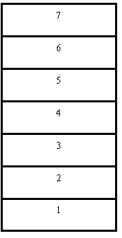
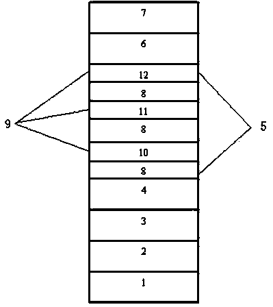
[0023] The preparation method of the epitaxial structure is to carry out high-temperature baking in the MOCVD reaction furnace to remove the residual impurities on the surface of the sapphire substrate 1, grow a layer of AlN buffer layer 2 after slowly cooling down at 500-900°C, and then rapidly raise the temperature, The U-shaped GaN layer 3 is grown at 900-1200° C. for about 10-80 minutes, with a thickness of 1-10 um. Afterwards, the N-type GaN layer 4 is grown at a growth temperature of 900-1200° C. and a growth thickness of 1-10 um. The active region 5 is grown, and P-AlGaN 6 is grown at 800-1000° C. to a thickness of 50-1000 Angstroms. Re-grow P-GaN 7 , the growth temperature is 800-1200°C, the thickness is 1000-5000 angstroms, and the concentration of Mg is 5x10 17 ~1x10 23 cm3.

[0024] The specific growth method of the active region of the present invention includes the following steps:

Embodiment 1

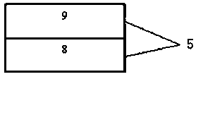
[0026]The active region 5 is grown for 3 cycles in nitrogen, hydrogen or a hydrogen-nitrogen mixed environment. The active region 5 includes three parts, and each part is grown for 1 cycle. The barrier layer consists of an AlxGa1-xN layer 10, an AlyIn1-yN layer 11 Composed of InzGa1-zN layers 12, the first part of the active region 5 is the alternate growth of well layers 8 and AlxGa1-xN layers 10; the second part of the active region 5 is the alternate growth of well layers 8 and AlyIn1-yN layers 11; the active region 5 The third part is the alternate growth of well layer 8 and InzGa1-zN layer 12. The growth temperature of the first part of the AlxGa1-xN layer 10 is 650 ° C, the Al composition is 017 cm 3 ; The growth temperature of the second part of the AlyIn1-yN layer 11 is 650°C, the Al composition is 017 cm 3 In the third part, the growth temperature of the InzGa1-zN layer 12 is 650°C, the In composition is 017 cm 3 .

Embodiment 2

[0028] The active region 5 is grown for 6 cycles in a nitrogen, hydrogen or hydrogen-nitrogen mixed environment. The active region 5 includes three parts, and each part is grown for 2 cycles. The barrier layer consists of an AlxGa1-xN layer 10, an AlyIn1-yN layer 11 Composed of InzGa1-zN layers 12, the first part of the active region 5 is the alternate growth of well layers 8 and AlxGa1-xN layers 10; the second part of the active region 5 is the alternate growth of well layers 8 and AlyIn1-yN layers 11; the active region 5 The third part is the alternate growth of well layer 8 and InzGa1-zN layer 12. The growth temperature of the first part of the AlxGa1-xN layer 10 is 850°C, the Al composition is 018 cm 3 ; The growth temperature of the second part AlyIn1-yN layer 11 is 800°C, the Al composition is 018 cm 3 In the third part, the growth temperature of the InzGa1-zN layer 12 is 800°C, the In composition is 018 cm 3 .


PUM

PropertyMeasurementUnit
Growth temperatureaaaaaaaaaa

Abstract

The invention discloses a blue-light LED (Light-Emitting Diode) epitaxial structure having an asymmetrical barrier layer, and relates to the technical field of epitaxy of light-emitting diodes. The structure comprises a sapphire substrate, an AlN (Aluminum Nitride) buffer layer, a U type GaN (Gallium Nitride) layer, an N type GaN layer, an active region, an electron blocking layer and a P type GaN layer in sequence from bottom to top, wherein the active region comprises a trap layer and a barrier layer; the growing period number of the active region is 3m; the active region comprises three parts, and each part grows for m periods; the barrier layer consists of an AlxGa1-xN layer, an AlyIn1-yN layer and an InzGa1-zn layer; and m is greater than or equal to 1 and smaller than or equal to 5. Compared with the prior art, the blue-light LED epitaxial structure has the advantages that an overflow phenomenon can be retarded, and bending of an energy band is reduced; and the internal quantum efficiency is increased, so that the light emitting efficiency is increased effectively.

Description

technical field [0001] The invention relates to the technical field of light-emitting diode epitaxy, in particular to a blue LED epitaxy structure with an asymmetric barrier layer. Background technique [0002] At present, as the global emphasis on new energy continues to increase, the LED industry is also developing rapidly. Many experts and scholars have developed many new materials and new structures that help improve brightness. Among them, the active region in the blue LED is a very important layer. [0003] In the prior art, the blue LED epitaxial structure includes a sapphire substrate 1, an AlN buffer layer 2, a U-type GaN layer 3, an N-type GaN layer 4, an active region 5, an electron blocking layer 6 and a P-type GaN layer 7, such as figure 1 shown. The active region 5 includes a well layer 8 and a barrier layer 9, such as figure 2 shown. However, the active region 5 of the above-mentioned structure has the following disadvantages: first, due to the large la...

Claims


Application Information

Patent Timeline
IPC IPC(8): H01L33/06
CPCH01L33/0075H01L33/06H01L33/12
Inventor 田宇郑建钦曾颀尧赖志豪郭廷瑞黄绣云黄信智张志刚吴东海童敬文林政志李鹏飞
Owner NANTONG TONGFANG SEMICON
Why Eureka
Try Eureka