GPP rectification chip based on reverse grooving technology

A technology of rectifying chips and reverse digging, which is applied in the direction of electrical components, electrical solid devices, circuits, etc., and can solve problems such as assembly difficulties, flashover, and two-electrode short circuits for subsequent customers

Inactive Publication Date: 2015-01-07
HUANGSHAN GUIDING ELECTRONICS
View PDF4 Cites 11 Cited by
  • Summary
  • Abstract
  • Description
  • Claims
  • Application Information

AI Technical Summary

Problems solved by technology

The disadvantage is that the negative angle structure of the product causes the equipotential lines to be dense on the edge, and the reverse withstand voltage that can be tolerated is not high. At present, it is difficult for the domestic GPP rectifier chip to exceed the level of 1600 volts
Another disadvantage is that the singleness of the reverse voltage is negative and positive, which makes it difficult for subsequent customers to assemble.
root tree figure 1 , the N-shaped surface of the product has a large area, and customers will weld this surface on the heat sink, which has a good heat conduction effect, while the P-shaped surface has a small area, which is used to connect with leads, conductive bars, etc. Forcibly welding the GPP rectifier chip upside down will not only cause poor thermal conductivity, but also cause accidents such as short circuit, breakdown, and flashover between the two electrodes.
As we all know, the electrical polarity of domestic bolted rectifiers is stipulated that the tube base is positive (should be connected to the P side of the chip), and the lead is negative (should be connected to the N side of the chip), so it is difficult to assemble GPP rectifier chips; a large number of automotive rectifiers Devices require half of the supply of rectifier chips with different polarities, forming a market blind spot in the promotion and application of GPP rectifier chips

Method used


Image

  • GPP rectification chip based on reverse grooving technology
  • GPP rectification chip based on reverse grooving technology
  • GPP rectification chip based on reverse grooving technology

Examples


Embodiment Construction

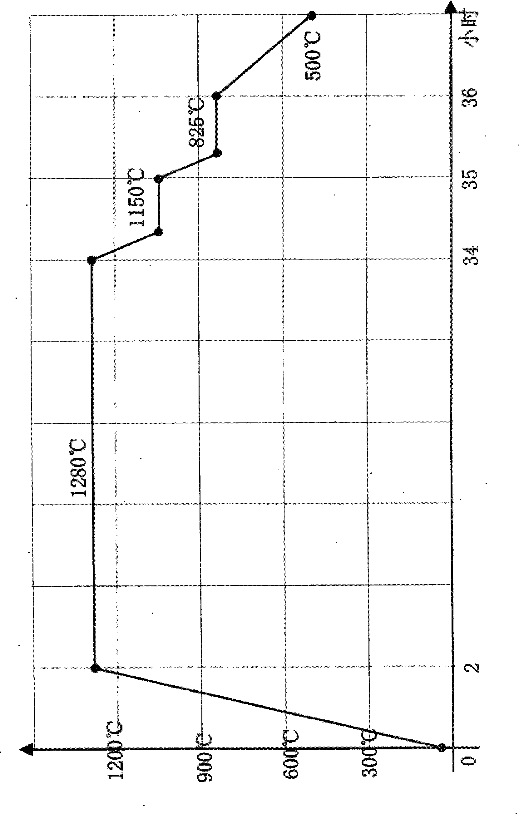
[0020] Mainly explain the formula and steps used in the implementation of the P-type impurity diffusion process in the process of producing GPP rectifier chips based on the back-grooving process:

[0021] The P-type diffusion impurity source formula is boric acid: aluminum nitrate: dehydrated alcohol, and the weight ratio is 9: 20: 80;

[0022] On the surface of the single crystal silicon wafer without phosphorus deposition, spin-coat the P-type diffusion impurity source, the equivalent coating amount is to coat 0.16 ml of phosphorus source solution on each side of each 3-inch single crystal silicon wafer, and the spin coating speed is 30 rpm Strictly control the reverse osmosis of the P-type diffusion impurity source to the phosphorus deposition surface. If there is a small amount of seepage on the edge of the phosphorus deposition surface, wipe it with a chemical fiber cloth dipped in absolute ethanol. The coated monocrystalline silicon wafer can be heated Plate or infrared ...


PUM


Abstract

The invention provides a new product of a GPP rectification chip based on the reverse grooving technology. The electric polarity of the GPP rectification chip is opposite to that of a conventional GPP rectification chip, the face, with a smaller area, in the up direction of the chip is the N type and the negative pole of the new product, and the face, with a larger area, in the down direction of the chip is the P type and the positive pole of the new product. The electric heating property of the new product is better than that of the conventional product, and the reveres withstand voltage is higher than 2000 volts. The production cost of the new product is not higher than that of the conventional product, so the new product can be produced through on-line equipment, instruments and materials of the conventional product, and requirements of customers for different polarities of rectification chip products can be met.

Description

technical field [0001] The R&D and production technology of GPP rectifier chips based on the back-digging process belongs to the field of "one-piece semiconductor device technology for new electronic components" in "High-tech Fields Supported by the State". Background technique [0002] At present, the production of domestic rectifier chips mostly adopts the "glass passivation protection" process, the so-called "GPP" process. The products produced - GPP rectifier chips (Glassivation Passivation Parts) have the advantages of no harmful and toxic substances, no heavy metal pollution in production, excellent electric heating performance, low manufacturing cost, and easy mass production. Due to the particularity of its structure and process, the GPP rectifier chip has its structural advantages and disadvantages. The following is an analysis based on the current production process and product structure. [0003] Take an N-type monocrystalline silicon wafer with diffusion to form...

Claims


Application Information

Patent Timeline
Patent Type & Authority Applications(China)
IPC IPC(8): H01L25/065
CPCH01L23/3178H01L2924/0002H01L2924/00
Inventor 程德明胡建业胡翰林汪华锋汪文锋
Owner HUANGSHAN GUIDING ELECTRONICS
Why Eureka
Try Eureka