Green-yellow light LED with doped wide potential barrier structure

A yellow-green light, potential barrier technology, applied in electrical components, circuits, semiconductor devices, etc., can solve problems such as low internal quantum efficiency, and achieve the effect of improving hole injection, improving product light efficiency, and improving product process window.

Active Publication Date: 2015-01-21
YANGZHOU CHANGELIGHT
View PDF4 Cites 12 Cited by
  • Summary
  • Abstract
  • Description
  • Claims
  • Application Information

AI Technical Summary

Problems solved by technology

[0006] The present invention can greatly improve the problem of low internal quantum efficiency of the traditional structure by adding a doped wide barrier structure layer in the active layer, improve the hole injection in the active region, and improve the electron-hole recombination efficiency, thereby greatly improving The light efficiency of the product, its brightness can

Method used


Image

  • Green-yellow light LED with doped wide potential barrier structure
  • Green-yellow light LED with doped wide potential barrier structure

Examples


Embodiment 1

[0014] 1. Production process steps:

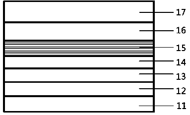
[0015] 1. Place the N-GaAs substrate 21 in the MOCVD reaction chamber, heat it to 600° C. to 700° C., remove the oxide layer on the substrate surface, and grow the GaAs buffer layer 22 .

[0016] 2. Growing a Bragg reflection layer 23 on the GaAs buffer layer 22 .

[0017] 3. Growing an N-type confinement layer 24 on the Bragg reflection layer 23 .

[0018] 4. Grow the first active layer 25 of non-doped superlattice on the N-type confinement layer 24: with Al X Ga (1-X) InP / Al Y Ga (1-Y) InP is the material, where X takes a value of 0.3, Y takes a value of 0.7, a period thickness of 10 nm, and a logarithm of 30 pairs.

[0019] 5. Al on the first active layer 25 Y Ga (1-Y) InP is used as a material, doped with impurities of the same conductivity type, and a wide barrier structure layer 26 is grown.

[0020] In this embodiment, the value of Y is 0.7, the thickness is 80nm, the doping element is Zn, and the doping concentration is 5E1...

Embodiment 2

[0033] 1. Production process steps:

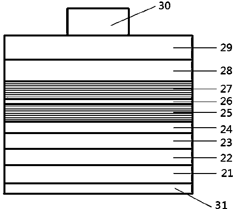
[0034] 1. Place the N-GaAs substrate 21 in the MOCVD reaction chamber, heat it to 600° C. to 700° C., remove the oxide layer on the substrate surface, and grow the GaAs buffer layer 22 .

[0035] 2. Growing a Bragg reflection layer 23 on the GaAs buffer layer 22 .

[0036] 3. Growing an N-type confinement layer 24 on the Bragg reflection layer 23 .

[0037] 4. Grow the first active layer 25 of non-doped superlattice on the N-type confinement layer 24: with Al X Ga (1-X) InP / Al Y Ga (1-Y) InP is the material, where X takes a value of 0.35, Y takes a value of 0.6, a period thickness of 10 nm, and a logarithm of 30 pairs.

[0038] 5. Al on the first active layer 25 Y Ga (1-Y) InP is used as a material, doped with impurities of the same conductivity type, and a wide barrier structure layer 26 is grown.

[0039] In this embodiment, the value of Y is 0.6, the thickness is 150 nm, the doping element is Mg, and the doping concentration is ...


PUM

PropertyMeasurementUnit
Thicknessaaaaaaaaaa
Dominant wavelengthaaaaaaaaaa

Abstract

The invention belongs to the technical field of photoelectrons, and relates to a green-yellow light LED with a doped wide potential barrier structure. The green-yellow light LED comprises a buffer layer, a bragg reflecting layer, a first limiting layer, a first non-doped superlattice active layer, a doped wide potential barrier structural layer, a second non-doped superlattice active layer, a second limiting layer and a GaP window layer, wherein the buffer layer grows on one face of a GaAs substrate. A first electrode is arranged on the GaP window layer. A second electrode is arranged on the other face of the GaAs substrate. According to the green-yellow light LED, the hole injection of the active area can be improved, the recombination efficiency of an electron hole is improved, accordingly, the product lighting effect can be greatly improved, the chip pass percent is increased by 2 percent to 4 percent, and therefore, a large number of high-efficiency and high-yield green-yellow light waveband LEDs with the light emitting wavelength ranging from 560 nm to 580 nm can be produced.

Description

technical field [0001] The invention belongs to the technical field of optoelectronics, and specifically relates to the technical field of AlGaInP quaternary system LED production. Background technique [0002] Quaternary AlGaInP yellow-green light-emitting diodes are widely used in various fields such as signal indication, display, traffic indication, display screen, automotive lighting, and special lighting. As the wavelength of quaternary AlGaInP materials shortens, the Al composition of the active layer increases continuously, and the combination of Al atoms with oxygen or carbon atoms leads to serious lattice defects in the material, and the luminous efficiency decreases; on the other hand, the energy band of yellow-green light is due to The proportion of Al component increases, the energy gap gradually changes from direct energy gap to indirect energy gap, and the internal quantum efficiency further drops significantly, resulting in low light efficiency of LED product...

Claims


Application Information

Patent Timeline
IPC IPC(8): H01L33/10H01L33/06
CPCH01L33/06H01L33/10
Inventor 林鸿亮李全素徐培强杨凯张双翔张银桥王向武李忠辉
Owner YANGZHOU CHANGELIGHT
Why Eureka
Try Eureka