Epitaxial wafer of GaN-based light-emitting diode and preparing method thereof

A technology of light-emitting diodes and epitaxial wafers, applied in electrical components, circuits, semiconductor devices, etc., can solve problems such as affecting the thermal stability of the device, reducing the crystal integrity, etc., to achieve good thermal stability of the device, improve service life, and good current. extended effect

Active Publication Date: 2015-01-21
HC SEMITEK SUZHOU
View PDF7 Cites 5 Cited by
  • Summary
  • Abstract
  • Description
  • Claims
  • Application Information

AI Technical Summary

Problems solved by technology

[0005] Although the uniformly doped current spreading layer has a low doping concentration, defects caused by doping (such as reducing the integrity of the crystal, etc.) will still occur, so there are still certain limitations in improving the internal quantum efficiency and reliability of LED devices. And because Si is an amphoteric impurity, when the doping amount in the N-type layer is relatively high, Si atoms will occupy the position of N atoms, forming a self-compensation effect, and the compensation ratio will also increase with the increase of Si doping concentration, Thus affecting the thermal stability of the device

Method used


Image

  • Epitaxial wafer of GaN-based light-emitting diode and preparing method thereof
  • Epitaxial wafer of GaN-based light-emitting diode and preparing method thereof

Examples


Embodiment 1

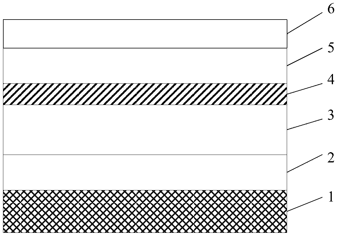
[0034] An embodiment of the present invention provides an epitaxial wafer of a GaN-based light emitting diode, see figure 1 , the epitaxial wafer includes a substrate 1, a buffer layer 2 grown on the substrate 1, an N-type layer 3, a multi-quantum well layer 5 and a P-type layer 6, and the epitaxial wafer also includes a layer grown on the N-type layer 3 and the multi-quantum well The N-type current spreading layer 4 between the layers 5, the N-type current spreading layer 4 is a GaN layer grown by delta doping technology, the doping concentration of the N-type current spreading layer 4 is lower than the doping concentration of the N-type layer 3, Starting from the N-type layer 3 side, the doping concentration of the N-type current spreading layer 4 remains constant or the doping concentration of the N-type current spreading layer 4 gradually decreases, and the N-type current spreading layer adjacent to the multi-quantum well layer 5 side The doping concentration of layer 4 is...

Embodiment 2

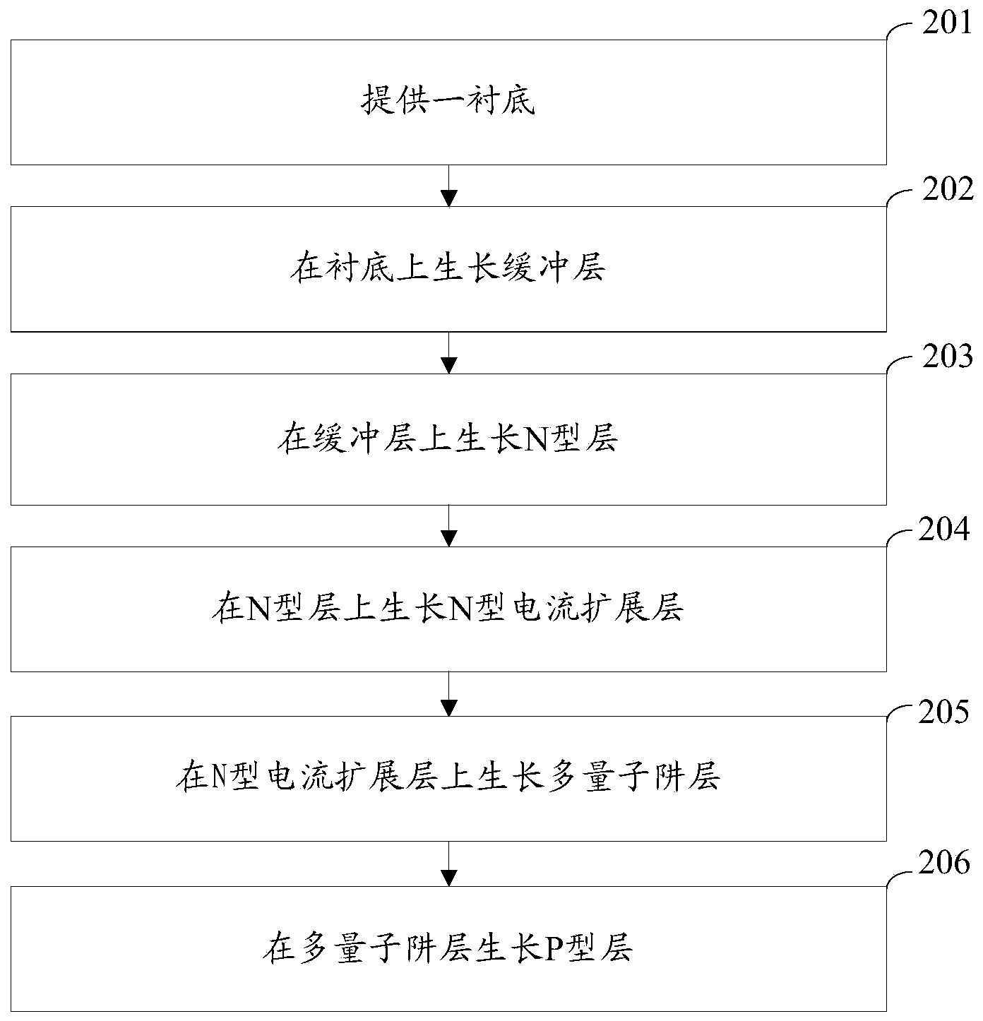
[0044] An embodiment of the present invention provides a method for preparing a GaN-based light-emitting diode, see figure 2 , the method includes:

[0045] Step 201: Provide a substrate.

[0046] Specifically, the substrate may be a sapphire substrate, and may also be a Si substrate or a SiC substrate.

[0047] Step 202: growing a buffer layer on the substrate.

[0048] Wherein, the buffer layer may be a composite layer, which may include a low-temperature buffer layer and an undoped GaN layer. Specifically, at a temperature of 540° C., a GaN layer with a thickness of 30 nm is grown on the substrate as a low-temperature buffer layer. Then the temperature is raised to about 1100°C, and a layer of undoped GaN layer with a thickness of about 3 μm is grown on the low-temperature buffer layer.

[0049] It is easy to know that before this step, the method may further include: cleaning the surface of the substrate. When it is realized, the sapphire substrate can be heated to 1...

Embodiment 3

[0077] The embodiment of the present invention provides a method for preparing a GaN-based light-emitting diode. The method for preparing the epitaxial wafer in this embodiment is basically the same as that in Embodiment 2, except that, starting from the side of the N-type layer, the N-type current expands The doping concentration of the layers decreases gradually.

[0078] Wherein, starting from the side of the N-type layer, the doping concentration of the N-type current spreading layer may decrease uniformly or irregularly. When it is realized, the time for feeding the doped impurity source can be uniformly or irregularly shortened each time without changing the flow rate of the impurity source, so as to gradually reduce the doping concentration of the N-type current spreading layer, and also Under the condition of not changing the time of feeding the impurity source each time, the flow rate of the impurity source can be reduced uniformly or irregularly, so as to gradually r...


PUM


Abstract

The invention discloses an epitaxial wafer of a GaN-based light-emitting diode and a preparing method of the epitaxial wafer, and belongs to the field of light-emitting diodes. The preparing method includes the steps that a substrate is provided; a buffer layer and an N-type layer sequentially grow on the substrate, an N-type current expanding layer, a multi-quantum-well layer and a P-type layer sequentially grow on the N-type layer, the N-type current expanding layer is a GaN layer adopting a delta doping technology for growth, the doping concentration of the N-type current expanding layer is smaller than that of the N-type layer, starting from one side of the N-type layer, the doping concentration of the N-type current expanding layer is kept unchanged or reduced gradually, and the doping concentration of the portion, adjacent to one side of the multi-quantum-well layer, of the N-type current expanding layer is zero. The current expanding layer grows by adopting the delta doping technology, the carrier concentration is high, compensation is small, and the device is good in heat stability; the undoped GaN layer is introduced into the position close to an active area to ensure transverse expansion of currents and reduce forward voltage drop, the service life is prolonged, and the fact that defects caused by doping extend to the active area and a non-radiative recombination center is reduced.

Description

technical field [0001] The invention relates to the field of light-emitting diodes, in particular to an epitaxial wafer of a GaN-based light-emitting diode and a preparation method thereof. Background technique [0002] LED (Lighting Emitting Diode, light-emitting diode) has the advantages of high efficiency, long life, small size, low power consumption, etc., and can be used for indoor and outdoor white lighting, screen display, backlighting, etc. In the development of this industry, GaN materials It is a typical representative of V-III compound semiconductors, so how to improve the photoelectric performance of GaN-based light-emitting diodes has become a key technology in the semiconductor lighting industry. [0003] The traditional GaN-based epitaxial wafer growth method is to grow an undoped GaN layer, an N-type layer, a multi-quantum well layer and a P-type layer sequentially on the substrate layer. Among them, the N-type layer is the main electron-supply layer, doped ...

Claims


Application Information

Patent Timeline
Patent Type & Authority Applications(China)
IPC IPC(8): H01L33/32H01L33/06
CPCH01L33/005H01L33/06H01L33/325H01L2933/0008
Inventor 李昱桦乔楠韩杰胡加辉魏世祯
Owner HC SEMITEK SUZHOU
Why Eureka
Try Eureka