Method for preparing high quality nitrides
A nitride, high-quality technology, applied in chemical instruments and methods, from chemical reactive gases, semiconductor/solid-state device manufacturing, etc., can solve problems such as unfavorable large-scale production, harsh environmental requirements, and complex processes, and achieve low cost The effect of growth, good material quality and simple process
- Summary
- Abstract
- Description
- Claims
- Application Information
AI Technical Summary
Problems solved by technology
Method used
Image
Examples
Embodiment 1
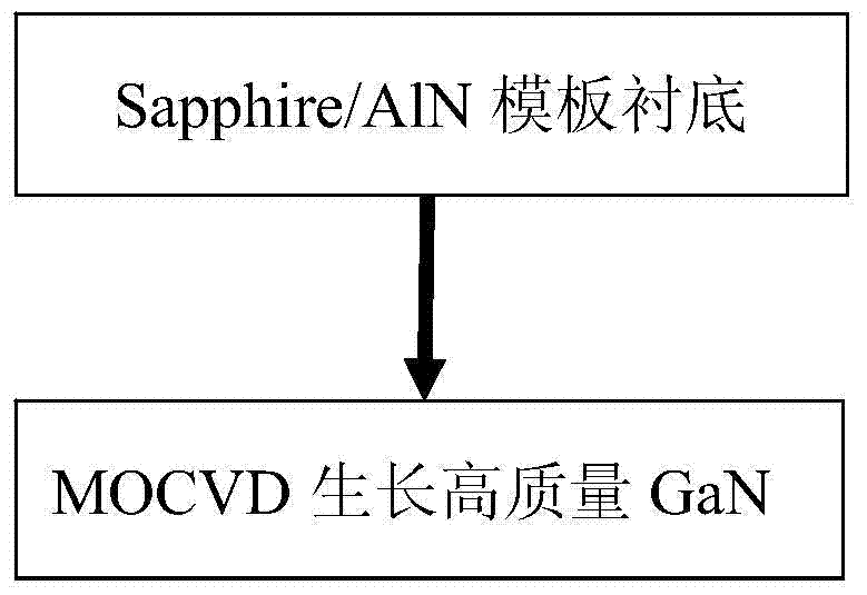
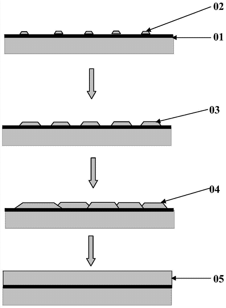
[0021] see figure 1 : This figure is a flowchart of the method for growing high-quality GaN on Sapphire / AlN templates, including:
[0022] (1) Sapphire / AlN template is used as the substrate material, and the lattice mismatch degree is 2.4%.
[0023] If the lattice mismatch between the substrate material and the epitaxial material is too small, the interfacial stress between the substrate material and the epitaxial material is too small, making the epitaxial layer tend to grow in a quasi-two-dimensional layer, and it is impossible to achieve "in situ Lateral epitaxial growth"; if the lattice mismatch between the epitaxial material and the substrate material is too large, the epitaxial material tends to grow in three-dimensional "islands", and the "islands" are difficult to merge into films. Therefore, the lattice mismatch between the substrate material and the epitaxial material should be moderate, not too large or too small, and the lattice mismatch is 0.5%-10%. The optimum ...
Embodiment 2
[0032] Methods for growing high-quality AlGaN epitaxial layers, including:
[0033] (1) Use Sapphire / AlN template, Si / AlN template or SiC / AlN template as the substrate material.
[0034] When the AlGaN epitaxial layer is grown directly on the Sapphire / AlN template, Si / AlN template or SiC / AlN template by MOCVD method, the lattice mismatch between the AlGaN epitaxial layer and the substrate material increases with the increase of the Al composition. reduce. For the Al composition in the range of 0.2-1, the lattice mismatch between the AlGaN epitaxial layer and the Sapphire / AlN template, Si / AlN template or SiC / AlN template is about 0.5%-2.4%.
[0035] (2) AlGaN epitaxial layer is grown by metal-organic chemical vapor deposition (MOCVD). The growth temperature of AlGaN epitaxial layer increases with the increase of Al composition. Preferably, for the Al composition in the range of 0.2-1, the growth temperature of AlGaN is 1050-1300°C. The growth process of the AlGaN epitaxial ...
Embodiment 3
[0038] Methods for growing high-quality InGaN epitaxial layers, including:
[0039] (1) Using Sapphire / GaN template, Si / GaN template, SiC / GaN template, Sapphire / AlN template, Si / AlN template or SiC / AlN template as the substrate material.
[0040] When the InGaN epitaxial layer is directly grown on the Sapphire / GaN template, Si / GaN template or SiC / GaN template by MOCVD method, the lattice mismatch between the InGaN epitaxial layer and the substrate material increases with the increase of the In composition. Increase. For the In composition within the range of 0.05-1, the lattice mismatch between the InGaN epitaxial layer and the Sapphire / GaN template, Si / GaN template or SiC / GaN template is about 0.5%-10%.
[0041] When the InGaN epitaxial layer is directly grown on the Sapphire / AlN template, Si / AlN template or SiC / AlN template by MOCVD method, the lattice mismatch between the InGaN epitaxial layer and the substrate material increases with the increase of the In composition. I...
PUM
 Abstract
Description
Claims
Application Information
 - R&D
- Intellectual Property
- Life Sciences
- Materials
- Tech Scout
- Unparalleled Data Quality
- Higher Quality Content
- 60% Fewer Hallucinations
Browse by: Latest US Patents, China's latest patents, Technical Efficacy Thesaurus, Application Domain, Technology Topic, Popular Technical Reports.
© 2025 PatSnap. All rights reserved.Legal|Privacy policy|Modern Slavery Act Transparency Statement|Sitemap|About US| Contact US: help@patsnap.com


