

Organic semiconductor material, preparation method thereof, and electroluminescent device
A technology of electroluminescent devices and organic semiconductors, which is applied in the field of organic semiconductor materials, preparation, and electroluminescent devices, can solve problems such as shortages, achieve high triplet energy levels, simple synthesis methods, and improve luminous efficiency.
- Summary
- Abstract
- Description
- Claims
- Application Information
AI Technical Summary
Problems solved by technology
Method used
Image

Examples
preparation example Construction
[0025] The invention provides a kind of preparation method of organic semiconductor material, comprises the steps:
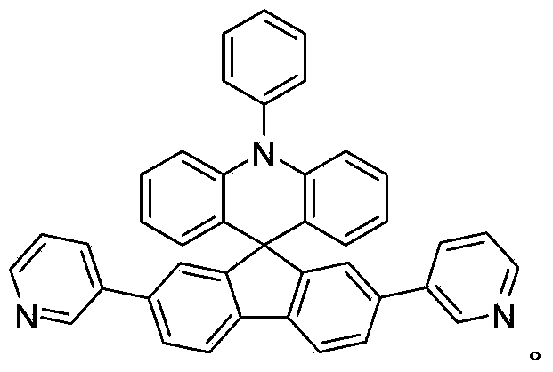
[0026] Provides compound A: and compound B: Under an inert atmosphere, add Compound A and Compound B into an organic solvent containing a catalyst and an alkali solution at a molar ratio of 1:2 to 1:2.4, and perform a Suzuki coupling reaction at 70 to 130°C for 12 to 48 hours, then stop the reaction The chemical formula to obtain the organic semiconductor material is as follows:
[0027]
[0028] The preparation method of the organic semiconductor material further includes a post-processing step, and the post-processing step is specifically: extracting the organic semiconductor material obtained by stopping the reaction with dichloromethane, combining the organic phases, drying them with anhydrous magnesium sulfate, and using petroleum A mixed solvent of ether and ethyl acetate was used as eluent, separated and purified through a silica gel layer, and dri...
Embodiment 1
[0041] The preparation process of 10-phenyl-2',7'-bis(pyridin-3-yl)-10H-spiro[acridine-9,9'-fluorene] The preparation steps are as follows:
[0042]
[0043] Under argon protection, 10-phenyl-2′,7′-bis(pinacol borate)-10H-spiro[acridine-9,9′-fluorene] (132mg, 0.2mmol), 3 -Bromopyridine (64mg, 0.4mmol) was added to a flask containing 10ml of toluene solvent, and after fully dissolving, potassium carbonate (2mL, 2mol / L) solution was added to the flask, vacuumed to remove oxygen and filled with argon, and then added Bistriphenylphosphinepalladium dichloride (5.6mg, 0.008mmol); the flask was heated to 100°C for Suzuki coupling reaction for 24h. The reaction was stopped and cooled to room temperature, extracted three times with dichloromethane, the organic phases were combined, dried over anhydrous magnesium sulfate and then spin-dried to obtain the 10-phenyl-2',7'-bis(pyridin-3-yl)-10H -Spiro[acridine-9,9'-fluorene] organic semiconductor material, and then use petroleum ether:...
Embodiment 2
[0048] The preparation process of 10-phenyl-2',7'-bis(pyridin-3-yl)-10H-spiro[acridine-9,9'-fluorene] The preparation steps are as follows:
[0049]
[0050] Under the protection of mixed gas of nitrogen and argon, 10-phenyl-2′,7′-bis(pinacol borate)-10H-spiro[acridine-9,9′-fluorene] (198mg, 0.3mmol ), 3-bromopyridine (114mg, 0.72mmol) and 12mL N,N-dimethylformamide were added into a 50mL two-necked flask, fully dissolved, and a mixture of nitrogen and argon was introduced to exhaust the air for about 20 minutes, and then the Tetrakistriphenylphosphine palladium (4mg, 0.003mmol) was added to it, and after fully dissolved, sodium bicarbonate (3mL, 2mol / L) solution was added. Then, the mixed gas of nitrogen and argon was exhausted for about 10 minutes, and the two-neck flask was added to 70°C for Suzuki coupling reaction for 48 hours. The reaction was stopped and cooled to room temperature, extracted three times with dichloromethane, the organic phases were combined, dried o...
PUM
 Abstract
Description
Claims
Application Information