Silicon-dioxide optical waveguide production process for manufacturing optical divider

A silicon dioxide, optical splitter technology, applied in the direction of optical waveguide, light guide, optics, etc., can solve the problems of affecting the mechanical properties and thermal stability of the optical splitter, obvious birefringence effect, and large residual stress of materials. , to achieve the effects of improving mechanical properties and thermal stability, small internal residual stress, and uniform refractive index

Inactive Publication Date: 2015-02-18
成都康特电子高新科技有限责任公司
View PDF3 Cites 4 Cited by
  • Summary
  • Abstract
  • Description
  • Claims
  • Application Information

AI Technical Summary

Problems solved by technology

Optical splitters are generally made on six materials, including lithium niobate, semiconductor compounds, silicon dioxide, silicon-on-insulator, polymers, and glass. Nowadays, optical splitters made of silicon dioxide waveguides have excessive residual stress inside the material. Large, the birefringence effect is obvious, and the structural parameters of the waveguide are poor, which affects the mechanical properties and thermal stability of the fabricated optical splitter

Method used


Image

  • Silicon-dioxide optical waveguide production process for manufacturing optical divider

Examples


Embodiment

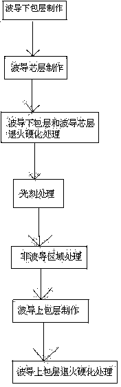
[0022] Such as figure 1 Shown, the present invention comprises the production technique for making the silicon dioxide optical waveguide of optical splitter, it is characterized in that, comprises the steps:

[0023] A. Fabrication of the lower cladding of the waveguide, using the flame hydrolysis method or chemical vapor deposition process, a layer of SiO2 is grown on the silicon wafer, and doped with phosphorus and boron ions as the lower cladding of the waveguide;

[0024] B. The waveguide core layer is made by flame hydrolysis or chemical vapor deposition process, and a layer of SiO2 is grown on the lower cladding layer as the waveguide core layer;

[0025] C. The waveguide lower cladding and waveguide core layer are annealed and hardened. Through the annealing and hardening process, the two layers of SiO2 grown in front become dense and uniform;

[0026] D. Photolithography treatment, protect the required waveguide pattern with photoresist;

[0027] E. For the non-waveg...

Embodiment 2

[0032] The preferred specific structure of this embodiment is as follows on the basis of the above embodiments: in step B, germanium ions are doped in the core layer of the waveguide. This layer is given the desired refractive index.

[0033] The lower cladding layer of the waveguide fabricated in step A, the core layer of the waveguide fabricated in step B, and the upper cladding layer of the waveguide fabricated in step F have the same thickness.

[0034] After the waveguide lower cladding layer and the waveguide core layer are annealed and hardened in step C, the refractive indices of the waveguide lower cladding layer and the waveguide core layer are uniform. The residual stress inside the material is further reduced, and the birefringence effect of the waveguide is reduced, so that the mechanical performance and thermal stability of the optical splitter made of the material are better.

[0035] After the annealing and hardening treatment of the upper cladding layer of th...


PUM


Abstract

The invention discloses a silicon-dioxide optical waveguide production process for manufacturing an optical divider. The silicon-dioxide optical waveguide production process includes a lower waveguide wrapping layer manufacturing step, a waveguide core layer manufacturing step, a lower waveguide wrapping layer and waveguide core layer annealing and hardening step, a photoetching step, a non-waveguide area treatment step, an upper waveguide wrapping layer manufacturing step and an upper waveguide wrapping layer annealing and hardening processing step. The lower waveguide wrapping layer manufacturing step includes growing a SiO2 layer on a silicon wafer by the flame hydrolysis method or the chemical vapor deposition process, and doping phosphorous and boron ions as a lower waveguide wrapping layer. The waveguide core layer manufacturing step includes growing another SiO2 layer on the lower wrapping layer as a waveguide core layer by the flame hydrolysis method or the chemical vapor deposition process. The lower waveguide wrapping layer and waveguide core layer annealing and hardening step includes adopting annealing and hardening to let the two SiO2 layers be compact and uniform; the photoetching step includes protecting required waveguide graphs with photoresist. The non-waveguide area processing step includes etching a non-waveguide area by the reactive ion etching process. The upper waveguide wrapping layer manufacturing step includes removing the photoresist, covering another SiO2 layer on the waveguide core layer again by the flame hydrolysis method or the chemical vapor deposition process and doping the boron and phosphorous ions as an upper waveguide wrapping layer. The upper waveguide wrapping layer annealing and hardening step is used for fining and compacting the SiO2 layer of the upper waveguide wrapping layer. According to the above theory, the optical divider manufactured by the silicon dioxide optical waveguide is low internal residual stress, insignificant in birefrigent effect and is good in mechanical performance and thermal stability.

Description

technical field [0001] The invention relates to the field of manufacturing optical splitters, in particular to a production process of silicon dioxide optical waveguides used for manufacturing optical splitters. Background technique [0002] Like the coaxial cable transmission system, the optical network system also needs to couple, branch, and distribute optical signals, which requires optical splitters to achieve. Optical splitter, also known as optical splitter, is one of the important passive devices in optical fiber links. input terminals and N output terminals. Optical splitters used in fiber optic CATV systems are generally 1×2, 1×3 and 1×N optical splitters composed of them. Optical splitters are generally made on six materials, including lithium niobate, semiconductor compounds, silicon dioxide, silicon-on-insulator, polymers, and glass. Nowadays, optical splitters made of silicon dioxide waveguides have excessive residual stress inside the material. Large, the b...

Claims


Application Information

Patent Timeline
Patent Type & Authority Applications(China)
IPC IPC(8): G02B6/13G02B6/132G02B6/134G02B6/136
CPCG02B6/13G02B6/132G02B6/134G02B6/136
Inventor 余波宗瑞朝黎林青晓英杜泽永
Owner 成都康特电子高新科技有限责任公司
Why Eureka
Try Eureka