A layered electrode matched with mg-si-sn-based thermoelectric elements and its connection process
A thermoelectric element, matching technology, applied in the manufacture/processing of thermoelectric devices, thermoelectric device junction lead-out materials, etc., can solve the problems of low performance of Si thermoelectric materials and difficulty in developing to the application stage, etc., and achieve simple process And reliable, good electrical property transition, reduce the effect of interface thermal stress
- Summary
- Abstract
- Description
- Claims
- Application Information
AI Technical Summary
Problems solved by technology
Method used
Image
Examples
Embodiment 1
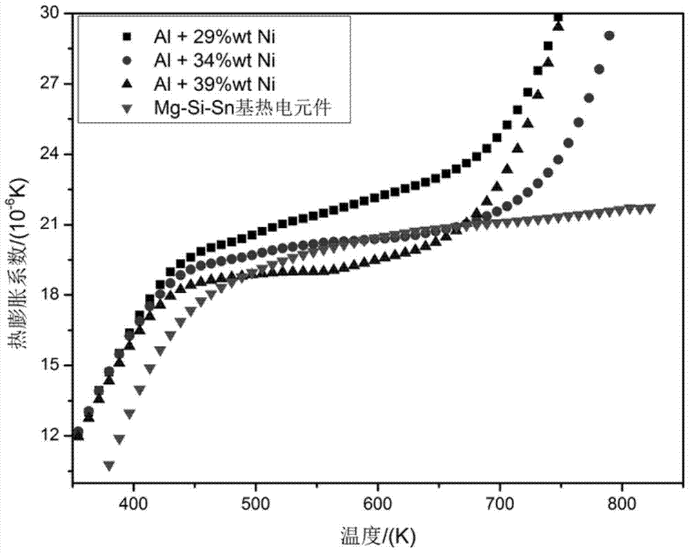
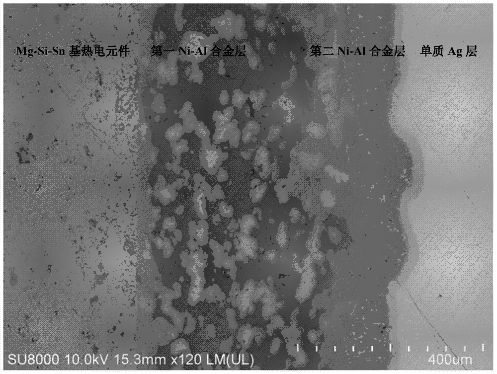
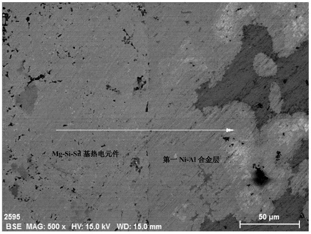
[0038] A multilayer electrode matched with a Mg-Si-Sn based thermoelectric element, the electrode is divided into a three-layer structure: first Ni-Al alloy layer, second Ni-Al alloy layer and elemental Ag layer. Wherein, the mass percent content of Ni element in the first Ni-Al alloy layer is 29%, the balance is Al element, and the thickness of the first Ni-Al alloy layer is 0.5mm; The Ni element in the second Ni-Al alloy layer The mass percentage is 42%, and the balance is Al element. The thickness of the second Ni-Al alloy layer is 0.15mm; the thickness of the simple Ag layer is 0.4mm.
[0039] The connection process of the multilayer electrode of the present invention and the Mg-Si-Sn base thermoelectric element is connected by spark plasma sintering (PAS), and the specific process steps are:
[0040] 1) Take 6.0g of Mg-Si-Sn-based thermoelectric material powder prepared by solid-state reaction, put it into a graphite mold for the first PAS sintering, the vacuum degree dur...
Embodiment 2
[0048] A multilayer electrode matched with a Mg-Si-Sn based thermoelectric element, the electrode is divided into a three-layer structure: first Ni-Al alloy layer, second Ni-Al alloy layer and elemental Ag layer. Wherein, the mass percent content of Ni element in the first Ni-Al alloy layer is 29%, the balance is Al element, and the thickness of the first Ni-Al alloy layer is 0.8mm; The Ni element in the second Ni-Al alloy layer The mass percentage is 59%, the balance is Al element, the thickness of the second Ni-Al alloy layer is 0.15mm; the thickness of the simple Ag layer is 0.6mm.
[0049] The connection process of the multilayer electrode of the present invention and the Mg-Si-Sn base thermoelectric element is connected by spark plasma sintering (PAS), and the specific process steps are:
[0050] 1) Take 6.0g of Mg-Si-Sn-based thermoelectric material powder prepared by solid-state reaction, put it into a graphite mold for the first PAS sintering, the vacuum degree during ...
Embodiment 3
[0058] A multilayer electrode matched with a Mg-Si-Sn based thermoelectric element, the electrode is divided into a three-layer structure: first Ni-Al alloy layer, second Ni-Al alloy layer and elemental Ag layer. Wherein, the mass percentage content of Ni element in the first Ni-Al alloy layer is 39%, the balance is Al element, and the thickness of the first Ni-Al alloy layer is 0.8mm; The Ni element in the second Ni-Al alloy layer The mass percentage content is 42%, the balance is Al element, the thickness of the second Ni-Al alloy layer is 0.15mm; the thickness of the simple Ag layer is 0.6mm.
[0059] The connection process of the multilayer electrode of the present invention and the Mg-Si-Sn base thermoelectric element is connected by spark plasma sintering (PAS), and the specific process steps are:
[0060] 1) Take 6.0g of Mg-Si-Sn-based thermoelectric material powder prepared by solid-state reaction, put it into a graphite mold for the first PAS sintering, the vacuum deg...
PUM
| Property | Measurement | Unit |
|---|---|---|
| thickness | aaaaa | aaaaa |
| thickness | aaaaa | aaaaa |
| thickness | aaaaa | aaaaa |
Abstract
Description
Claims
Application Information


