Low-temperature ceramic package process method of diode

A technology of low-temperature ceramics and packaging technology, which is applied in the fields of electrical components, semiconductor/solid-state device manufacturing, and circuits. Improve heat dissipation and high temperature resistance, reduce void rate, and achieve good thermal matching effects

Inactive Publication Date: 2018-11-13
YANTAI TAIXIN ELECTRONICS TECH CO LTD
View PDF5 Cites 1 Cited by
  • Summary
  • Abstract
  • Description
  • Claims
  • Application Information

AI Technical Summary

Problems solved by technology

[0003] At present, the TO series of high-power semiconductor devices generally use epoxy resin plastic packaging technology. Traditional plastic packaging devices use high-pressure injection molding machines to heat the epoxy resin at high temperature to soften it into a fluid state and inject it under pressure. The lead frame is wrapped inside, which is likely to cause injection molding voids and affect the heat dissipation of the product. The advantages of this type of product are simple process and low cost. The disadvantages are that the product has poor high temperature resistance, humidity resistance and salt spray resistance, and low reliability. It is mainly used in home appliances. low power field

Method used


Image

  • Low-temperature ceramic package process method of diode
  • Low-temperature ceramic package process method of diode
  • Low-temperature ceramic package process method of diode

Examples


specific Embodiment approach

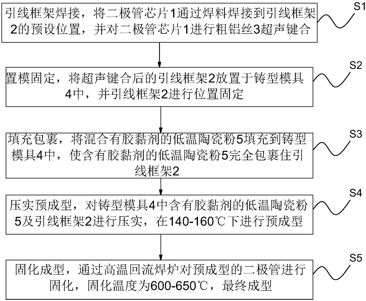
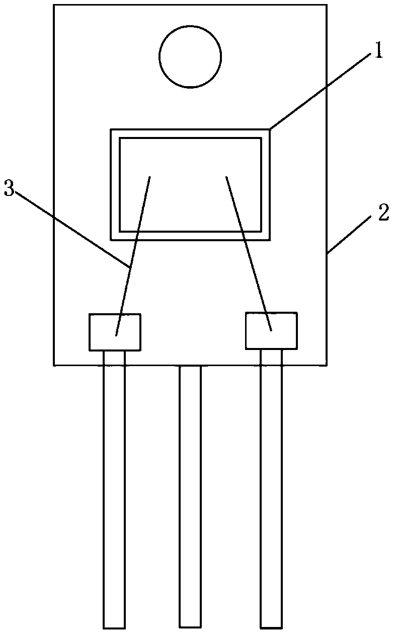
[0034] 1) Weld the Schottky diode chip 1 to the design position of the TO-264 lead frame 2DIE through high-temperature solder, and perform ultrasonic bonding on the diode chip 1 with thick aluminum wire 3, see figure 2 ;

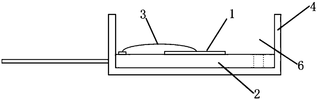
[0035] 2) Place the ultrasonically bonded lead frame 2 in the casting mold 4, and fix the position of the lead frame 2, see image 3 ;

[0036] 3) Fill the low-temperature ceramic powder 5 mixed with the adhesive into the casting mold 4, so that the low-temperature ceramic powder 5 containing the adhesive completely wraps the lead frame 2, see Figure 4 ;

[0037] 4) compacting the low-temperature ceramic powder 5 containing adhesive in the casting mold 4 and the lead frame 2, and preforming at 150° C.;

[0038] 5) The preformed diode is cured in a high-temperature reflow oven at a curing temperature of 600-650° C. for final molding.

[0039] Adopting the low-temperature ceramic powder forming and curing process of the present invention, since the ceram...


PUM

PropertyMeasurementUnit
particle diameteraaaaaaaaaa

Abstract

The invention discloses a low-temperature ceramic package process method of a diode. The low-temperature ceramic package process method comprises the steps of welding a diode chip at a preset positionof a lead frame by a welding material, and performing rough aluminum wire ultrasonic bonding on the diode chip; placing the lead frame in a casting die after ultrasonic bonding, and fixing the position of the lead frame; filling low-temperature ceramic powder mixed with an adhesive in the casting die so that the lead frame is completely wrapped by the low-temperature ceramic powder mixed with theadhesive; compacting the adhesive-containing low-temperature ceramic powder and the lead frame in the casting die, and performing pre-formation under 140-160 DEG C; and curing the pre-formed diode bya high-temperature reflow soldering furnace, and finally forming the diode, wherein the curing temperature is 600-650 DEG C. The processing product can conform to higher temperature application range, is high in cooling ability, can bear larger current and voltage load and has good moisture-resistant and salt mist-resistant capability, and the application requirement of high-end field of new energy, power systems, military projects and the like is met.

Description

technical field [0001] The invention relates to a diode low-temperature ceramic packaging process method, in particular to the packaging of TO series products of high-power semiconductor devices, and belongs to the technical field of diode packaging. Background technique [0002] A diode, also known as a crystal diode, is an electronic component that transmits current in only one direction. It is a device with two terminals joined by one part number, and has the property of making current flow or not flow according to the direction of the applied voltage. A crystal diode is a p-n junction formed by a p-type semiconductor and an n-type semiconductor, and a space charge layer is formed on both sides of the interface, and a self-built electric field is built. When there is no external voltage, the diffusion current caused by the carrier concentration difference on both sides of the p-n junction is equal to the drift current caused by the self-built electric field, and it is in ...

Claims


Application Information

Patent Timeline
Patent Type & Authority Applications(China)
IPC IPC(8): H01L21/329
CPCH01L29/6609
Inventor 姜维宾孙叔翔徐冰金浩
Owner YANTAI TAIXIN ELECTRONICS TECH CO LTD
Why Eureka
Try Eureka