Check patentability & draft patents in minutes with Patsnap Eureka AI!

Green-light LED (Light Emitting Diode) epitaxial layer structure and growing method

A growth method and epitaxial layer technology, applied in electrical components, circuits, semiconductor devices, etc., can solve the problems of weakening LED luminous intensity, increasing electron leakage, reducing electron injection efficiency, etc., to reduce polarization electric field intensity, improve Luminous efficiency, the effect of reducing the QCSE effect

Active Publication Date: 2015-03-04
INST OF SEMICONDUCTORS - CHINESE ACAD OF SCI
View PDF5 Cites 7 Cited by
  • Summary
  • Abstract
  • Description
  • Claims
  • Application Information

AI Technical Summary

Problems solved by technology

Although reducing the barrier height (such as using a single InGaN barrier) can effectively improve the hole injection efficiency and suppress the QCSE effect, but because the blocking effect of the potential barrier on electrons is reduced at the same time, the leakage of electrons is increased and the electron leakage is reduced. The injection efficiency will also lead to the weakening of LED luminous intensity

Method used


Image

  • Green-light LED (Light Emitting Diode) epitaxial layer structure and growing method
  • Green-light LED (Light Emitting Diode) epitaxial layer structure and growing method
  • Green-light LED (Light Emitting Diode) epitaxial layer structure and growing method

Examples


Embodiment Construction

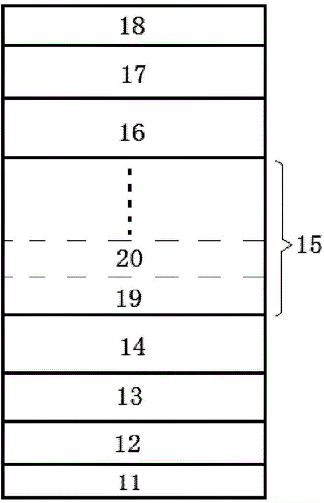
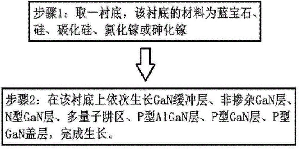
[0027] For a green LED epitaxial layer structure provided by the present invention, please refer to figure 1 shown, including:

[0028] A substrate 11, the material of the substrate 11 is sapphire, silicon, silicon carbide, gallium nitride or gallium arsenide;

[0029] a GaN buffer layer 12 grown on the substrate 11;

[0030] a non-doped GaN layer 13 grown on the GaN buffer layer 12;

[0031] An N-type GaN layer 14 grown on the non-doped GaN layer 13 . The thickness of the N-type GaN layer 14 is 1-3 μm, wherein the doping concentration of Si is greater than 10 18 / cm 3 ;

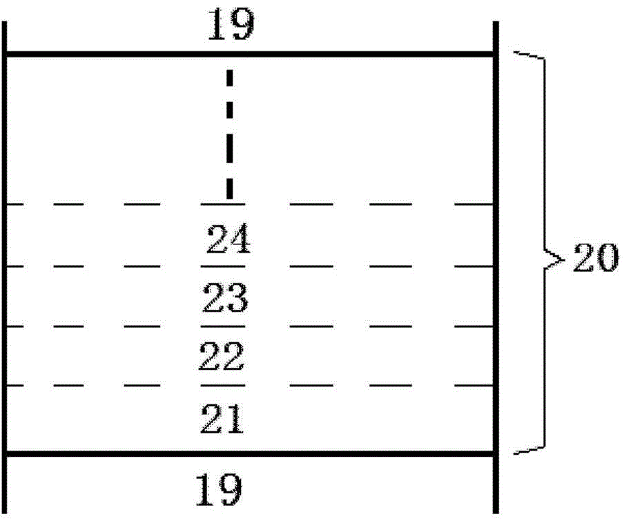
[0032] A multi-quantum well region 15 is grown on the N-type GaN layer 14 .

[0033] A P-type AlGaN layer 16 is grown on the multiple quantum well region 15 . The thickness of the layer is 30-50nm, the Al content is 5%-10%, and the P-type Mg doping concentration is greater than 10 18 / cm 3 ;

[0034] A P-type GaN layer 17, which is grown on the P-type AlGaN layer 16, the thickness of this layer is ...


PUM


Abstract

The invention discloses a green-light LED (Light Emitting Diode) epitaxial layer structure and a growing method. The green-light LED epitaxial layer structure comprises a substrate which is made of sapphire, silicon, silicon carbide, gallium nitride or gallium arsenide, a gallium nitride buffer layer which grows on the substrate, a non-doping gallium nitride layer which grows on the gallium nitride buffer layer, an N type gallium nitride buffer layer which grows on the non-doping gallium nitride layer, a multi-quantum-well area which grows on the N type gallium nitride layer, a P type aluminum gallium nitride layer which grows on the multi-quantum-well area, a P type gallium nitride layer which grows on the P type aluminum gallium nitride layer and a P type gallium nitride layer which grows on the P type gallium nitride layer. The green-light LED epitaxial layer structure achieves improvement of the LED luminous efficiency by improving the hole injection efficiency in a MQW (Multiple Quantum Well) and reducing the QCSE effect in an indium gallium nitride quantum well.

Description

technical field [0001] The invention belongs to the technical field of semiconductors, and in particular relates to a green LED epitaxial layer structure and a growth method, which can be used in the manufacture of semiconductor optoelectronic devices. Background technique [0002] GaN-based green light-emitting diode (LED) is a semiconductor solid-state light-emitting device widely used in the field of display and lighting. The core part of its epitaxial structure is the InGaN / GaN multiple quantum well (MQW) layer. The luminous efficiency of LED mainly depends on the structure and quality of the MQW layer, and optimizing the MQW structure and improving the quality of the MQW material is the fundamental way to obtain high-brightness green LED devices. [0003] In traditional GaN-based green LEDs, the simple structure of the InGaN / GaN MQW layer is used as the active region, which is characterized by the use of GaN material as the barrier layer to confine carriers. The struct...

Claims


Application Information

Patent Timeline
Patent Type & Authority Applications(China)
IPC IPC(8): H01L33/12H01L33/06H01L33/00
CPCH01L33/0075H01L33/06H01L33/12H01L33/14
Inventor 刘炜赵德刚陈平刘宗顺朱建军江德生
Owner INST OF SEMICONDUCTORS - CHINESE ACAD OF SCI
Features
  • R&D
  • Intellectual Property
  • Life Sciences
  • Materials
  • Tech Scout
  • Unparalleled Data Quality
  • Higher Quality Content
  • 60% Fewer Hallucinations
Learn More