Silicon wafer and wet etching system

A wet etching, silicon wafer technology, used in sustainable manufacturing/processing, electrical components, climate sustainability, etc., can solve problems such as poor appearance of solar cells, damage to diffusion surfaces, and unstable exhaust air, achieving increased Effective light-receiving area, improving photoelectric conversion rate, and eliminating redundant etched areas

Inactive Publication Date: 2015-03-11
ZHEJIANG JINKO SOLAR CO LTD +1
View PDF4 Cites 4 Cited by
  • Summary
  • Abstract
  • Description
  • Claims
  • Application Information

AI Technical Summary

Problems solved by technology

The RENA Inoxiside chain wet etching machine uses a single-sided wet etching process, which makes the silicon wafer float on the chemical solution to etch side N-type silicon. However, the silicon wafer floats on the chemical solution. Liquid tension and immersion into the edge diffusion surface will inevitably affect the N-type silicon on the diffusion surface, which is an unavoidable defect in wet etching
[0004] At present, the RENA Ionxiside chain wet etching machine can control the width of the single-sided etching line at 0.5mm~1.0mm. The wider the etching line width, the larger the area of ​​the redundant etching area, and the effective light-receiving area of ​​the battery will decrease. Reduced, resulting in a decrease in open circuit voltage and short circuit current, and a decrease in cell efficiency
On the other hand, in the RENA Inoxiside chain wet etching machine, due to the bubble explosion in the reaction tank and the splashing of the etching solution, the dripping of the condensed etching solution above the tank, the unstable exhaust, and the abnormal flow rate, etc., caused The diffusion surface is damaged by the etching solution, which eventually leads to the appearance of various solar cells with poor appearance and electrical performance failure.

Method used


Image

  • Silicon wafer and wet etching system
  • Silicon wafer and wet etching system

Examples


Embodiment 1

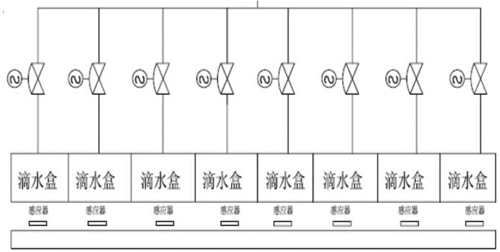
[0030] 1. Install a constant pressure tank on the RENA equipment, and connect a separate water pipe to the constant pressure tank on the original pure water main road;

[0031] 2. Install eight drip boxes above the etching section of the RENA equipment, connect the eight water outlets of the constant pressure tank to the drip boxes, and the eight drip boxes are divided into eight channels; install sensors in charge of eight channels above the driving roller of the feeding table, Add an encoder to the equipment transmission system to measure the transmission speed;

[0032] 3. Install a PP electrical box near the feeding end on the side of the equipment, and install an independent PLC inside the electrical box to form a water film spray system.

[0033] The above water film sprinkler system is a control system independent of RENA equipment. When the sensor detects that the silicon wafer to be etched enters the loading table, it sends a signal to the PLC, and the PLC performs d...

Embodiment 2

[0035] 1. Install a constant pressure tank on the RENA equipment, and connect a separate water pipe to the constant pressure tank on the original pure water main road;

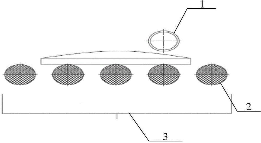
[0036] 2. Install eight drip boxes above the etching section of the RENA equipment, connect the eight water outlets of the constant pressure tank to the drip boxes, and the eight drip boxes are divided into eight channels; install sensors in charge of eight channels above the driving roller of the feeding table, An encoder is added to the equipment transmission system to measure the transmission speed; a pressure roller is installed on the feeding table corresponding to the drip box to make it roll the water film dripping on the surface of the silicon wafer to make it more uniform, and at the same time A diversion box is added to the lower part of the pressure water roller to discharge the squeezed water film; figure 2 as shown, figure 2 Schematic diagram of the structure of the pressurized rollers added to...


PUM


Abstract

The invention provides a silicon wafer, comprising a to-be-etched silicon wafer and a water film protecting layer compounded on the diffusion surface of the to-be-etched silicon wafer. The water film protecting layer formed on the diffusion surface of the to-be-etched silicon wafer is used for protecting the silicon wafer in the subsequent etching, so that chemical liquids cannot enter the diffusion surface of the silicon wafer in the subsequent wet etching process and excessive etching regions generated in the wet etching process can be removed; the effective light interception area of PN junctions can be increased and the photoelectric conversion efficiency can be improved. The invention further provides a wet etching system, comprising a water film spraying system arranged at the feeding end of wet etching equipment.

Description

technical field [0001] The invention relates to the technical field of wet etching in the solar cell manufacturing process, in particular to a silicon wafer and a wet etching system. Background technique [0002] A solar cell is a device that directly converts light energy into electrical energy through the photoelectric effect or photochemical effect. The most widely used solar cells are silicon solar cells. The manufacturing process of silicon solar cells is as follows: texturing, diffusion, etching, PEVCD, screen printing, sintering and testing. In the above-mentioned manufacturing process, since the edge of the battery after the silicon wafer is diffused, there will be N-type impurities and the P-type substrate to form a PN junction, and a thick phosphosilicate glass layer is formed on the surface of the battery during the diffusion process, so the silicon wafer needs to be The edges and surfaces are etched. [0003] RENA Inoxiside wet etching is the most common etchi...

Claims


Application Information

Patent Timeline
Patent Type & Authority Applications(China)
IPC IPC(8): H01L21/67H01L31/18
CPCY02P70/50
Inventor 黄华蒋方丹金浩陈康平
Owner ZHEJIANG JINKO SOLAR CO LTD
Why Eureka
Try Eureka