High-reliability image sensor packaging structure with stress protection structure

A technology of image sensor and protective structure

Inactive Publication Date: 2015-03-11
BEIJING UNIV OF TECH
View PDF4 Cites 4 Cited by
  • Summary
  • Abstract
  • Description
  • Claims
  • Application Information

AI Technical Summary

Problems solved by technology

[0004] However, in the current image sensor packaging, there are still many problems that affect product reliability:
The material used for the support wall 2 is generally a polymer material. Since the thermal expansion coefficients of the cover plate 1, the wafer 4, and the support wall 2 are quite different, the mismatch of the thermal expansion coefficients will lead to thermal stress. occur, causing the packaging structure to be prone to delamination and cracks between the support wall and the cover plate 1 and the wafer 4 during the follow-up reliability test and service, resulting in a decline in the function of the device or even failure; in addition, because the support wall 2 has A certain height, which increases the overall thickness of the package structure, affects the final dimensions of the product, especially in the direction of thickness.
[0006] 2. Since there are many different materials in the packaging structure, and the thermal expansion coefficients of each material are different, this leads to the occurrence of thermal stress due to the mismatch of thermal expansion coefficients during the service of the device
Since the area to be cut contains a variety of materials with different hardness, such as redistribution circuit layer, silicon, polymer, cover plate 1, etc., this poses a great challenge to the cutting process, and it is easy to generate fragments, slivers, etc.
On the other hand, during the subsequent service of the packaged product, since the metal layer 8 is in direct contact with the outside world around the package structure, once delamination occurs between the interfaces, it is easy to introduce moisture from the external environment into the package structure , resulting in accelerated failure of the device

Method used


Image

  • High-reliability image sensor packaging structure with stress protection structure
  • High-reliability image sensor packaging structure with stress protection structure
  • High-reliability image sensor packaging structure with stress protection structure

Examples


Embodiment Construction

[0037] The present invention will be described in more detail below with reference to accompanying drawing:

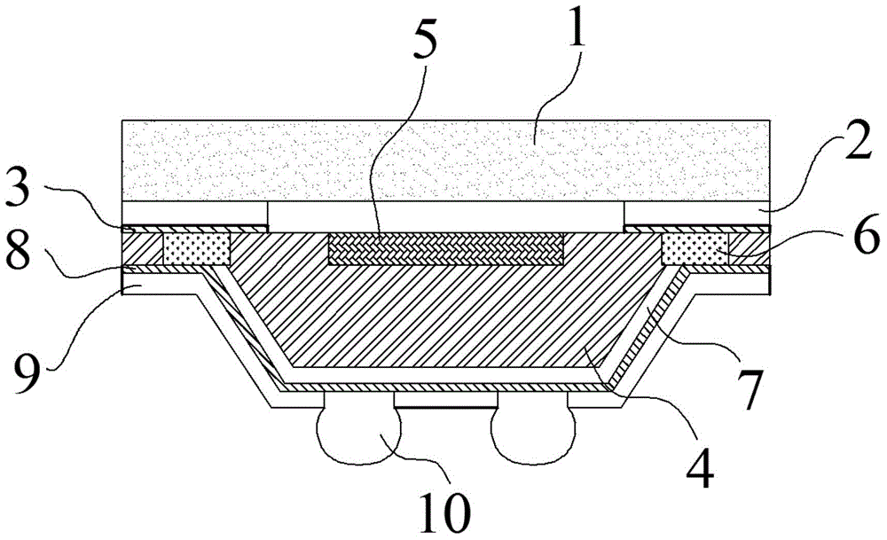
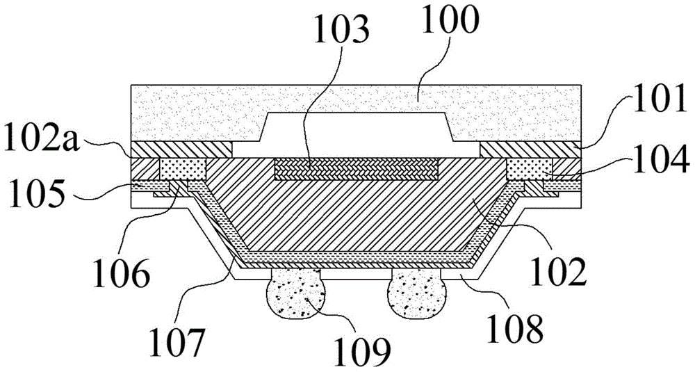
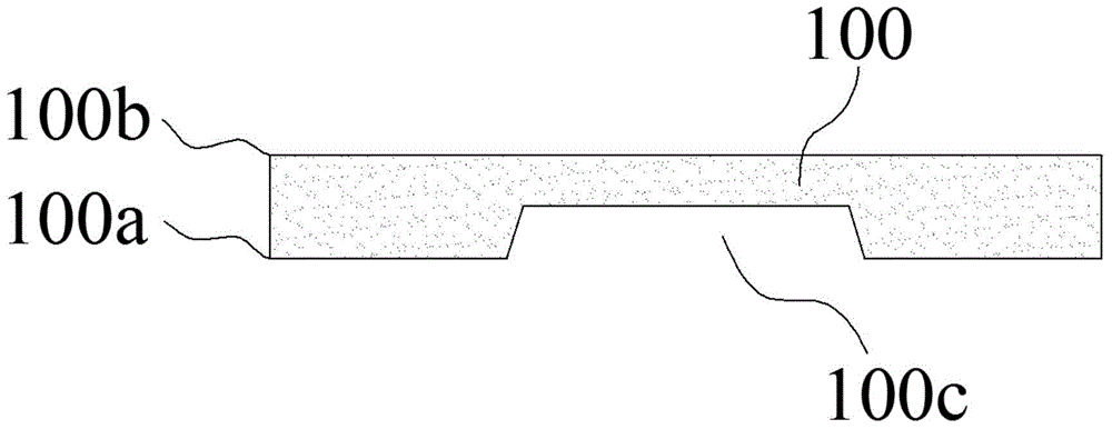
[0038] As shown in FIG. 1(b), a high-reliability image sensor package with a stress protection structure according to an embodiment of the present invention includes: 1. a cover plate 100, and a cavity structure 100c is fabricated on the front surface 100a of the cover plate; 2. .wafer 102, which comprises wafer front 102a and wafer back 102b; 3. image sensing area 103 and bonding pad 104, and described image sensing area 103 and bonding pad 104 are all distributed on wafer front 102a, wherein welding The disc 104 is distributed around the image sensing area 103, and realizes conduction; 4. The bonding glue 101 is located between the cover plate 100 and the wafer 102, and the two are bonded together; 5. The redistribution circuit layer, A passivation layer 105, a metal layer 107, and a solder resist layer 108 are sequentially formed on the back side of the wafer 102b. ...


PUM


Abstract

The invention discloses a high-reliability image sensor packaging structure with a stress protection structure and belongs to the field of image sensor packaging. The high-reliability image sensor packaging structure comprises a cover plate, a wafer, an image sensing area, welding discs, bonding glue, a passivation layer, a metal layer and a solder mask layer, a cavity structure is formed on the front of the cover plate, the wafer comprises a wafer front and a wafer back, both the image sensing area and the welding discs are distributed on the wafer front, the welding discs are distributed around the image sensing area and realize breakover, the bonding glue is positioned between the cover plate and the wafer and bonds the same together, and the passivation layer, the metal layer and the solder mask layer are sequentially formed on the back of the wafer. Breakover between the welding discs on the front of the wafer and solder balls on the back of the wafer is realized through a redistribution line layer formed by the above structure. Thickness of the packaging structure is lowered, stress in the metal layer is reduced, cutting process yield is increased, and packaging reliability is improved.

Description

technical field [0001] The invention relates to a high-reliability image sensor packaging structure with a stress protection structure and a method for manufacturing the packaging structure, belonging to the field of image sensor packaging. Background technique [0002] An image sensor is a semiconductor module, a device that converts an optical image into an electronic signal that can be used for further processing, digitized and stored, or used to transfer the image to another display device for display Wait. It is widely used in digital cameras and other electro-optical devices. Image sensors are now mainly divided into charge-coupled devices (CCD) and CMOS image sensors (CIS, CMOS Image Sensor). Although the CCD image sensor is superior to the CMOS image sensor in terms of image quality and noise, the CMOS sensor can be manufactured with traditional semiconductor production technology, and the production cost is relatively low. At the same time, due to the relatively ...

Claims


Application Information

Patent Timeline
Patent Type & Authority Applications(China)
IPC IPC(8): H01L27/146
Inventor 秦飞武伟安彤肖智轶
Owner BEIJING UNIV OF TECH
Why Eureka
Try Eureka