Low subthreshold swing high withstand voltage insulated gate tunneling transistor and method of making the same

A technology of tunneling transistors and insulating gates, which is applied in the field of ultra-large-scale integrated circuit manufacturing, can solve the problems of increasing production costs, increasing process difficulty, and cannot substantially improve the tunneling probability of silicon materials, and achieves good forward withstand voltage. and the effect of reverse withstand voltage characteristics

Inactive Publication Date: 2017-05-24
SHENYANG POLYTECHNIC UNIV
View PDF3 Cites 0 Cited by
  • Summary
  • Abstract
  • Description
  • Claims
  • Application Information

AI Technical Summary

Problems solved by technology

However, this approach not only increases the production cost, but also increases the difficulty of the process.
In addition, the use of high dielectric constant insulating materials as the insulating dielectric layer between the gate and the substrate can only improve the control ability of the gate to the electric field distribution of the channel, but cannot essentially increase the tunneling probability of silicon materials, so The improvement of electrical characteristics such as sub-threshold slope conduction current is very limited

Method used


Image

  • Low subthreshold swing high withstand voltage insulated gate tunneling transistor and method of making the same
  • Low subthreshold swing high withstand voltage insulated gate tunneling transistor and method of making the same
  • Low subthreshold swing high withstand voltage insulated gate tunneling transistor and method of making the same

Examples


Embodiment Construction

[0048] Below in conjunction with accompanying drawing, the present invention will be further described:

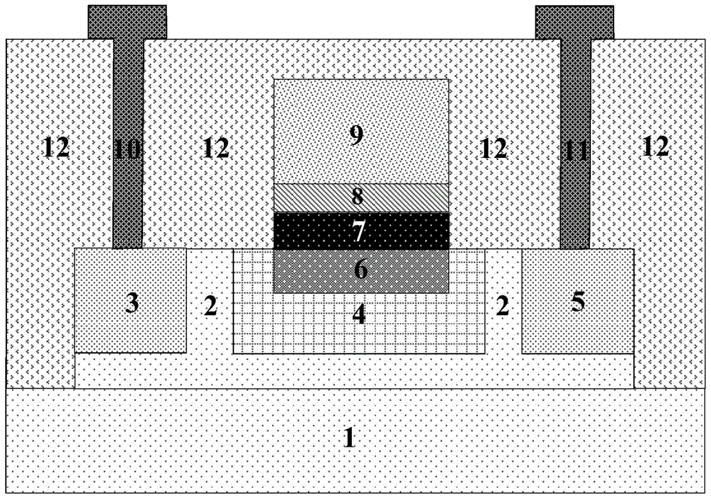
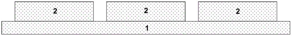
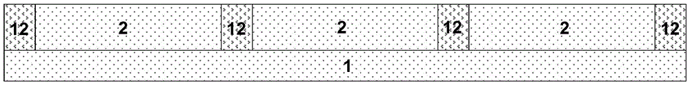
[0049] like figure 1 It is a schematic diagram of a two-dimensional structure of a low subthreshold swing high withstand voltage insulated gate tunneling transistor formed on a bulk silicon substrate in the present invention; it specifically includes a single crystal silicon substrate 1; a withstand voltage layer 2; an emitter region 3; a moderately doped Impurity base region 4; collector region 5; heavily doped base region 6; conductive layer 7; tunnel insulating layer 8; gate electrode 9; emitter 10; collector 11; blocking insulating layer 12.

[0050] Low sub-threshold swing high withstand voltage insulated gate tunneling transistor, the substrate 1 uses a single crystal silicon wafer as the substrate for forming the device, or uses an SOI wafer as the substrate for forming the device; a withstand voltage layer 2 is formed above the substrate The emitter region 3, the ...


PUM


Abstract

The invention relates to a low sub-threshold swing high withstand voltage insulated gate tunneling transistor. A withstand voltage layer structure with low impurity concentration is introduced into the collector junction and the emitter junction to improve the forward and reverse withstand voltage capabilities of the device. The extremely sensitive correlation between the resistance through the insulating layer and the electric field strength in the tunneling insulating layer enables lower subthreshold swing and better switching characteristics. By using the tunneling current generated on the insulating tunneling layer as the driving current of the collector current, better forward current conduction characteristics are achieved compared with common semiconductor band-to-band tunneling field effect transistors. The invention also proposes a specific manufacturing method of the low sub-threshold swing high withstand voltage insulated gate tunneling transistor. Therefore, the working characteristic of the nanoscale integrated circuit unit is significantly improved, and it is suitable for popularization and application.

Description

[0001] Technical field: [0002] The invention relates to the field of ultra-large-scale integrated circuit manufacturing, and relates to a low subthreshold swing, high withstand voltage insulating gate tunneling transistor and a manufacturing method thereof, which are suitable for manufacturing high-performance ultra-high integrated integrated circuits. [0003] Background technique: [0004] At present, the continuous shortening of the channel length of integrated circuit unit metal oxide semiconductor field effect transistors (MOSFETs) has led to the increase of the subthreshold swing of the device, which has brought about serious degradation of switching characteristics and a significant increase in static power consumption, etc. short channel effect. Although the degradation of the device performance can be alleviated by improving the gate electrode structure, when the device size is further reduced to below 50 nm, even with the optimized gate electrode structure, the subt...

Claims


Application Information

Patent Timeline
Patent Type & Authority Patents(China)
IPC IPC(8): H01L29/739H01L29/423H01L29/06H01L21/335
CPCH01L29/0684H01L29/66409H01L29/772
Inventor 靳晓诗刘溪
Owner SHENYANG POLYTECHNIC UNIV
Why Eureka
Try Eureka