Method for forming semiconductor structure

A technology of semiconductor and gate structure, which is applied in the field of formation of semiconductor structures, can solve the problems of increased difficulty of FinFET process and performance degradation of FinFET, and achieves the effect of stable and accurate performance and precise feature size

Active Publication Date: 2015-03-18
SEMICON MFG INT (SHANGHAI) CORP
View PDF5 Cites 8 Cited by
  • Summary
  • Abstract
  • Description
  • Claims
  • Application Information

AI Technical Summary

Problems solved by technology

[0004] However, as the process node shrinks, the difficulty of forming the fin field effect transis

Method used


Image

  • Method for forming semiconductor structure
  • Method for forming semiconductor structure
  • Method for forming semiconductor structure

Examples


Embodiment Construction

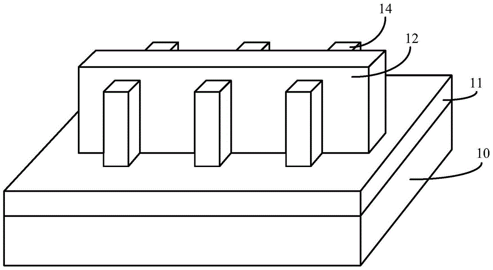
[0028] As mentioned in the background art, in the prior art, the process of forming a fin field effect transistor is relatively difficult, and the formed fin field effect transistor has poor performance.

[0029] As the process node shrinks, the size of the fins and the distance between adjacent fins also shrink accordingly, resulting in poor quality of the gate dielectric layer and gate electrode layer formed on the sidewalls and top surfaces of the fins. Please continue to refer figure 1 The method for forming a gate structure on the surface of the fin in the prior art includes: using a deposition process to form a gate dielectric film on the surface of the dielectric layer 11, and the sidewall and top surface of the fin 14; forming a gate electrode on the surface of the gate dielectric film Thin film: using an anisotropic dry etching process to etch part of the gate electrode film and gate dielectric film until the top and sidewall surfaces of the fin 14 and the surface of ...


PUM


Abstract

A method for forming a semiconductor structure comprises the following steps: a substrate is provided, wherein the surface of the substrate is provided with a mask layer which exposes part of the surface of the substrate; part of the substrate is etched with the mask layer as a mask, openings are formed in the substrate, and a fin part is formed on the substrate between every two adjacent openings; after the fin parts are formed, the size of the mask layer in the direction parallel to the surface of the substrate is reduced to enable the mask layer to expose part of the top surfaces of the fin parts; and after the size of the mask layer in the direction parallel to the surface of the substrate is reduced, the fin parts are etched with the mask layer as a mask and by a directional etching process to make the side walls of the fin parts inclined relative to the surface of the substrate and the top size of the fin parts smaller than the bottom size. The size of a semiconductor structure formed by the method is accurate and easy to control, and the performance of a fin type field effect transistor formed by the semiconductor structure is improved.

Description

technical field [0001] The invention relates to the technical field of semiconductor manufacturing, in particular to a method for forming a semiconductor structure. Background technique [0002] With the rapid development of semiconductor manufacturing technology, semiconductor devices are developing towards higher element density and higher integration. As the most basic semiconductor device, transistors are currently being widely used. Therefore, with the increase of component density and integration of semiconductor devices, the gate size of planar transistors is getting shorter and shorter. The ability of traditional planar transistors to control channel current Weakened, resulting in short channel effect, resulting in leakage current, and ultimately affecting the electrical performance of semiconductor devices. [0003] In order to overcome the short channel effect of the transistor and suppress the leakage current, the prior art proposes a Fin Field Effect Transistor ...

Claims


Application Information

Patent Timeline
IPC IPC(8): H01L21/336H01L21/28
CPCH01L21/28H01L29/66795
Inventor 张翼英何其暘
Owner SEMICON MFG INT (SHANGHAI) CORP
Why Eureka
Try Eureka