Fin-type field effect transistor and formation method thereof

A fin-type field effect and transistor technology, which is applied in semiconductor devices, semiconductor/solid-state device manufacturing, electrical components, etc., can solve the problem that the carrier mobility cannot be satisfied.

Active Publication Date: 2015-03-18
SEMICON MFG INT (SHANGHAI) CORP
View PDF3 Cites 12 Cited by
  • Summary
  • Abstract
  • Description
  • Claims
  • Application Information

AI Technical Summary

Problems solved by technology

[0006] The problem solved by the invention is that with the expansion of information data in modern society, faster and more eff...

Method used


Image

  • Fin-type field effect transistor and formation method thereof
  • Fin-type field effect transistor and formation method thereof
  • Fin-type field effect transistor and formation method thereof

Examples


Embodiment Construction

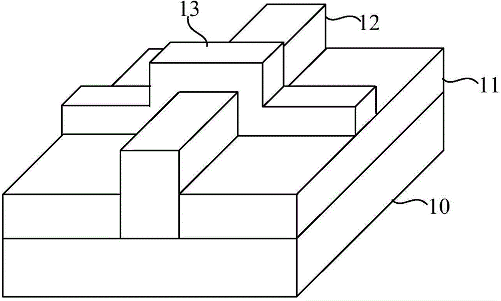
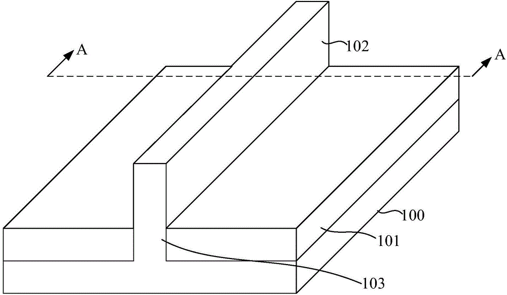
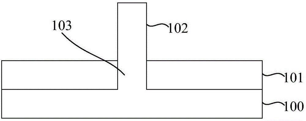
[0064] Pure graphene is a new type of carbonaceous thin film material that is densely packed into a two-dimensional honeycomb structure by a single layer of carbon atoms. Graphene is not only the thinnest known material, but also very strong and hard; as a single substance, graphene can transfer electrons faster than known conductors at room temperature, so good electrical properties make graphene very useful in the field of semiconductor technology has great potential value.

[0065] For a conventional FinFET, the region serving as the channel region is a semiconductor material with a certain energy gap. However, graphene has no energy gap, which has become an obstacle to the application of graphene in the field of semiconductor technology. The present invention just aims at this and proposes a method for forming a fin field effect transistor with graphene. In the method for forming, graphene is hydrogenated so that graphene becomes a "semiconductor material" with an energy ...


PUM


Abstract

Disclosed are a fin-type field effect transistor and a formation method thereof. The formation method of the fin-type field effect transistor includes the following steps: providing a substrate and forming a fin part on the substrate; forming a silicon-carbon layer on the surface of the fin part; carrying out thermal decomposition on the silicon-carbon layer so that the silicon-carbon layer of a part thickness or all thickness is changed into a graphene layer; carrying out hydrotreating on the graphene layer so that a hydrogen-containing energy gap structure is formed on the surface layer of the graphene layer; forming a gate dielectric layer on the graphene layer and forming a first gate electrode which crosses the gate dielectric layer on the gate dielectric layer; removing the gate dielectric layer and the graphene layer at the two ends of the fin part and forming epitaxial layers with doping on the surface of the exposed fin part, wherein the epitaxial layers and the first gate electrode are separated by the remaining gate dielectric layer and the graphene layer and the epitaxial layers with doping at the two ends of the fin part are used respectively as a source electrode and a drain electrode. The hydrogen-containing energy gap structure introduces an energy gap into the graphene layer and the graphene layer with the hydrogen-containing energy gap structure is used as a channel area so that the mobility ratio of carriers in the transistor is improved.

Description

technical field [0001] The invention relates to the technical field of semiconductors, in particular to a fin field effect transistor and a forming method thereof. Background technique [0002] In the field of semiconductor technology, with the continuous reduction of the feature size of integrated circuits and the requirement for higher signal transmission speed of integrated circuits, transistors need to have higher driving current while gradually reducing their size. To meet this requirement, the length of conventional complementary metal oxide semiconductor (CMOS) transistors has become shorter than before, however, it is still difficult to meet the requirements of high integration. [0003] Therefore, in the prior art, a Fin Field Effect Transistor (FinFET) has been proposed. refer to figure 1 The fin field effect transistor comprises: an insulating layer 11 located on a substrate 10; a fin 12 penetrating through the insulating layer 11 and higher than the upper surfa...

Claims


Application Information

Patent Timeline
IPC IPC(8): H01L29/78H01L21/336
CPCH01L29/66795H01L29/785
Inventor 张海洋
Owner SEMICON MFG INT (SHANGHAI) CORP
Why Eureka
Try Eureka