Pyroelectric infrared detector sensing unit and manufacturing method thereof

A pyroelectric infrared and sensitive unit technology, which is applied in the direction of electrical components, final product manufacturing, sustainable manufacturing/processing, etc., can solve the problem of difficult to prepare high-performance pyroelectric infrared detectors, weak absorption layer adhesion, Process incompatibility and other issues, to achieve the effect of excellent heat transfer performance, small specific heat capacity, and firm adhesion

Active Publication Date: 2015-03-25
UNIV OF ELECTRONIC SCI & TECH OF CHINA
View PDF3 Cites 3 Cited by
  • Summary
  • Abstract
  • Description
  • Claims
  • Application Information

AI Technical Summary

Problems solved by technology

[0005] At present, the absorption layer of pyroelectric infrared detectors has disadvantages such as weak adhesion or narrow absorption b

Method used


Image

  • Pyroelectric infrared detector sensing unit and manufacturing method thereof
  • Pyroelectric infrared detector sensing unit and manufacturing method thereof

Examples


example 1

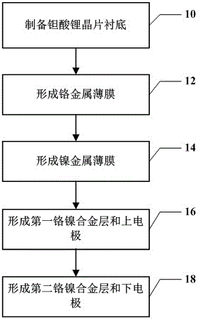
[0048] (1) Lithium tantalate (LiTaO 3 ) crystal surface treatment

[0049] 1) Cleaning LiTaO 3 wafer. to LiTaO 3 Surface A (first surface) and surface B (second surface) of the wafer are mechanically thinned and polished and chemically etched. Wet etching LiTaO 3 Wafer to remove defects and damage caused by thinning polishing.

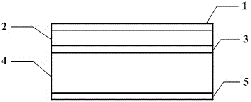
[0050] (2) Depositing an infrared absorbing layer and etching to form an electrode structure

[0051] 2) Clean LiTaO 3 The wafer is photolithographically patterned on the A side (that is, the pattern described above is formed).

[0052] 3) In LiTaO 3 Chromium metal film and nickel metal film are deposited on the A side of the wafer by magnetron sputtering process. Float cleaning. Among them, the thickness of the chromium metal film is 15nm, and the thickness of the nickel metal film is 60nm.

[0053] 4) In LiTaO 3 Photolithographic patterning of the A side of the wafer.

[0054] 5) In LiTaO 3 The magnetron sputtering process was used to d...

example 2

[0061] (1) LiTaO 3 surface treatment

[0062] 1) Cleaning LiTaO 3 wafer. to LiTaO 3 Surface A (first surface) and surface B (second surface) of the wafer are mechanically thinned and polished and chemically etched. Wet etching LiTaO 3 Wafer to remove defects and damage caused by thinning polishing.

[0063] (2) Deposit the infrared absorbing layer and etch to form the electrode structure

[0064] 2) Clean LiTaO 3 The wafer is photolithographically patterned on the A side.

[0065] 3) In LiTaO 3 Chromium metal film and nickel metal film are deposited on the A side of the wafer by magnetron sputtering process, and the float cleaning is carried out. Among them, the thickness of the chromium metal film is 20nm, and the thickness of the nickel metal film is 65nm.

[0066] 4) In LiTaO 3 Photolithographic patterning of the A side of the wafer.

[0067] 5) In LiTaO 3 The chromium-nickel alloy absorption layer was deposited on the A side of the wafer by thermal evaporation...


PUM

PropertyMeasurementUnit
Thicknessaaaaaaaaaa
Thicknessaaaaaaaaaa
Thicknessaaaaaaaaaa

Abstract

The embodiment of the invention discloses a manufacturing method of a pyroelectric infrared detector sensing unit. The manufacturing method includes the steps that a lithium tantalite wafer substrate is manufactured; a chromium metallic film is formed on the first surface of the lithium tantalite wafer substrate; a nickel metallic film is formed on the chromium metallic film; a first chrome-nickel alloy layer is formed on the nickel metallic film, and an upper electrode is formed through etching; a second chrome-nickel alloy layer is formed on the second surface of the lithium tantalite wafer substrate, and a lower electrode is formed through etching. An absorbing layer of the pyroelectric infrared detector sensing unit manufactured through the method has the advantages of being good in repeatability, high in absorptivity, small in specific heat capacity and excellent in heat transfer performance, attachment is firm, the absorbing wave band is wide, the spectrum is flat, and the absorbing layer can simultaneously serve as an electrode and therefore is suitable for serving as the absorbing layer of the pyroelectric infrared detector sensing unit.

Description

technical field [0001] The invention relates to the technical field of pyroelectric infrared detectors, in particular to a pyroelectric infrared detector sensitive unit and a manufacturing method thereof. [0002] Background technique [0003] Pyroelectric infrared detectors have many advantages such as room temperature operation, low power consumption, compact structure, high reliability, wide and flat spectral response, simple process, low price, and strong anti-interference, and can be widely used in military defense, industrial , medicine and health, environmental monitoring and scientific research and other fields, such as infrared guidance and intrusion alarm, safety monitoring, fire alarm, industrial production monitoring, aircraft volume assisted driving, medical diagnosis, spectral analysis, earth atmosphere monitoring and many other aspects. [0004] When the infrared radiation is incident on the pyroelectric infrared detector, the infrared radiation is absorbed b...

Claims


Application Information

Patent Timeline
IPC IPC(8): H01L31/101H01L31/18
CPCH01L31/101H01L31/109H01L31/18Y02P70/50
Inventor 刘子骥梁志清王涛黎威志于贺王军
Owner UNIV OF ELECTRONIC SCI & TECH OF CHINA
Why Eureka
Try Eureka