Structured arrangement manometer coarsened sapphire substrate and preparation method
A sapphire substrate, nanotechnology, applied in the direction of electrical components, circuits, semiconductor devices, etc., can solve the problem of low light extraction efficiency of GaN-based LEDs, achieve enhanced light extraction efficiency and light output power, high light extraction efficiency, and improve light The effect of the probability of escape
- Summary
- Abstract
- Description
- Claims
- Application Information
AI Technical Summary
Problems solved by technology
Method used
Image

Examples
Embodiment 1
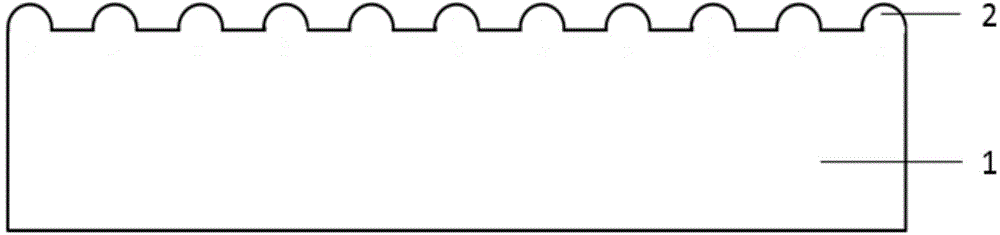
[0041] (1) Deposit a layer of silicon dioxide mask on the sapphire substrate; coat a layer of photoresist on the mask layer, use ICP equipment to etch the mask layer to form a mask pattern, and use a mixed solution of sulfuric acid and phosphoric acid Wet etched sapphire. A micron-scale figure 1 is prepared; the micron-scale figure is a truncated cone, the height of which is 1.5 μm, and the diameter of the bottom surface is 2 μm.
[0042] (2) The substrate is cleaned, and then a silicon dioxide film with a thickness of 200 nm is deposited on the micron-scale pattern 1 .
[0043] (3) Clean the substrate, then deposit a silver film with a thickness of 100nm on the silicon dioxide film, and anneal in the air at a temperature of 250 degrees for 1000 seconds, so that the silver film is agglomerated into nanoparticles.
[0044] (4) transfer the nanoparticle pattern to the silicon dioxide film by ICP dry etching pattern transfer method, and use sulfur hexafluoride as the etching gas. ...
Embodiment 2
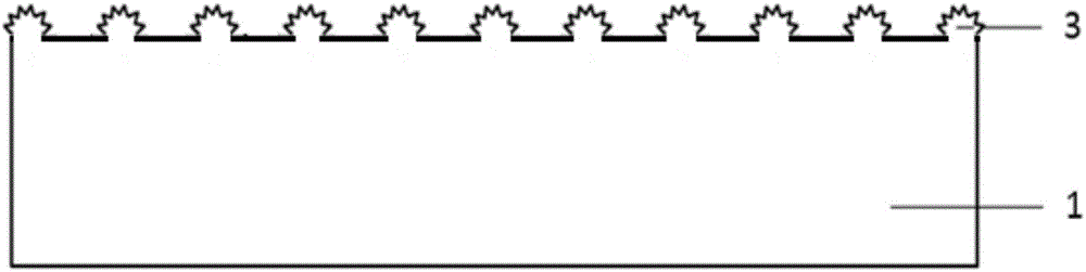
[0049] (1) Deposit a layer of silicon dioxide mask on the sapphire substrate; coat a layer of photoresist on the mask layer, use ICP equipment to etch the mask layer to form a mask pattern; use a mixed solution of sulfuric acid and phosphoric acid Wet etched sapphire. Micron-scale pattern 1 is prepared; the micron-scale pattern is a square prism, the height of the pattern is 10 μm, the diameter of the bottom surface (ie, the longest diagonal line of the bottom surface) is 10 μm, and the shortest diagonal line of the bottom surface is 6 μm.
[0050] (2) The substrate is cleaned, and then a silicon dioxide film with a thickness of 1000 nm is deposited on the micron-scale pattern 1 .
[0051] (3) Re-deposit a silver film with a thickness of 200nm on the silicon dioxide film in step (2); anneal in oxygen at a temperature of 900 degrees for 5000s to make the silver film agglomerate and become nanoparticles.
[0052] (4) transfer the nanoparticle pattern to the silicon dioxide film...
Embodiment 3
[0057] (1) Deposit a layer of silicon dioxide mask on the sapphire substrate; coat a layer of photoresist on the mask layer, use ICP equipment to etch the mask layer to form a mask pattern; use a mixed solution of sulfuric acid and phosphoric acid Wet etched sapphire. Micron-scale pattern 1 is prepared; the micron-scale pattern is a pentagonal prism with a height of 10 μm and a bottom diameter of 25 μm (the diameter of the bottom surface of the prism, that is, its longest diagonal).
[0058] (2) depositing a silicon dioxide film with a thickness of 500nm on the micron-scale pattern formed in step (1);
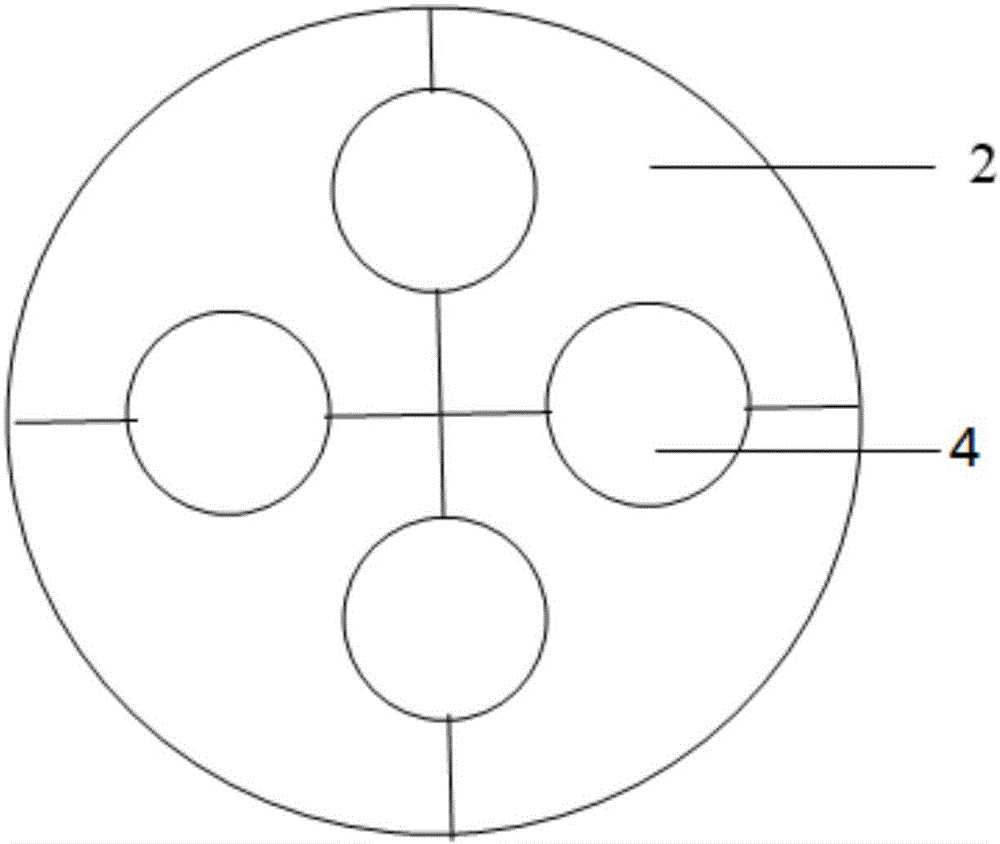
[0059] (3) Re-deposit a silver film with a thickness of 300nm on the silicon dioxide film of step (2); anneal in air at a temperature of 2000 degrees for 200s to make the silver film agglomerate and become nanoparticles. Experiments have shown that the silver nanoparticles prepared under this condition have a pattern height of 500nm and a bottom diameter of 20nm.
[0060] (4)...
PUM
| Property | Measurement | Unit |
|---|---|---|
| Height | aaaaa | aaaaa |
| Bottom diameter | aaaaa | aaaaa |
| Height | aaaaa | aaaaa |
Abstract
Description
Claims
Application Information
 - R&D
- Intellectual Property
- Life Sciences
- Materials
- Tech Scout
- Unparalleled Data Quality
- Higher Quality Content
- 60% Fewer Hallucinations
Browse by: Latest US Patents, China's latest patents, Technical Efficacy Thesaurus, Application Domain, Technology Topic, Popular Technical Reports.
© 2025 PatSnap. All rights reserved.Legal|Privacy policy|Modern Slavery Act Transparency Statement|Sitemap|About US| Contact US: help@patsnap.com