
Photonic crystal all-optical OR conversion logic gate

A technology of photonic crystals and two-dimensional photonic crystals, applied in the direction of logic circuits using optoelectronic devices, logic circuits, logic circuits using specific components, etc., can solve problems such as large volume and difficult production, and achieve strong anti-interference ability and structural Compact, easy-to-make effects

Inactive Publication Date: 2015-04-01
SHENZHEN UNIV
View PDF4 Cites 2 Cited by
  • Summary
  • Abstract
  • Description
  • Claims
  • Application Information

AI Technical Summary

Problems solved by technology

These optical logic devices have the common disadvantage of large volume for the development of large-scale integrated optical circuits
With the improvement of science and technology in recent years, people have also developed quantum optical logic devices, nanomaterial optical logic devices and photonic crystal optical logic devices. These logic devices all meet the size requirements of large-scale photonic integrated optical circuits, but for modern In terms of manufacturing technology, quantum optical logic devices and nanomaterial optical logic devices have great difficulties in manufacturing, while photonic crystal optical logic devices have a competitive advantage in manufacturing technology

Method used


Image

  • Photonic crystal all-optical OR conversion logic gate
  • Photonic crystal all-optical OR conversion logic gate
  • Photonic crystal all-optical OR conversion logic gate

Examples


Embodiment Construction

[0025] Below in conjunction with accompanying drawing and specific embodiment the present invention is described in further detail:

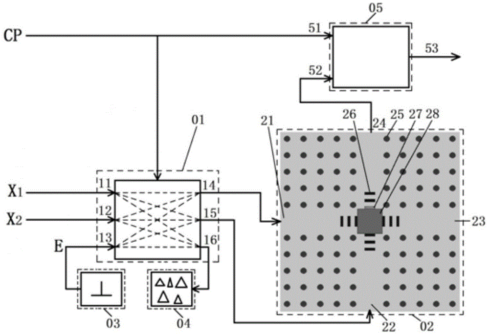
[0026] Such as figure 1 As shown, the photonic crystal all-optical or conversion logic gate of the present invention is composed of an optical switch unit 01, a photonic crystal structure unit 02, a reference light source 03, a wave-absorbing load 04 and a D flip-flop unit 05; the optical switch unit 01 is a 3×3 optical gating switch controlled by the clock signal CP, which is used to control the output of the selection logic signal. The optical gating switch controls the three input signals through the clock signal CP to select the output as the next-level photon The logic input of the crystal structure unit; the optical gating switch is composed of a clock signal CP input terminal, two system signal input terminals, a reference optical input terminal and three intermediate signal output terminals, and the two system signal input terminals are ...


PUM

PropertyMeasurementUnit
refractive indexaaaaaaaaaa

Abstract

The invention discloses a photonic crystal all-optical OR conversion logic gate which comprises a photonic crystal structural unit, an optical switch unit, a reference light source, a wave-absorbing load and a D trigger unit, wherein two system signal input ends of the optical switch unit are connected with a logic signal X1 and a logic signal X2; the reference light source is connected with a reference light input end of the optical switch unit; three middle signal output ends of the optical switch unit are respectively connected with two middle signal input ends of the photonic crystal structural unit and the wave-absorbing load; a clock control signal CP is connected with a clock signal CP input end of the optical switch unit and a clock signal input end of the D trigger unit through the input ends of a two-branch waveguide; the output end of the photonic crystal structural unit is connected with a D signal input end of the D trigger unit. The photonic crystal all-optical OR conversion logic gate has the advantages of compact structure, high operating rate, high anti-jamming capability and easiness in integration with other optical logic elements.

Description

technical field [0001] The invention relates to two-dimensional photonic crystals, optical or logic gates Background technique [0002] In 1987, E. Yablonovitch of Bell Laboratories in the United States was discussing how to suppress spontaneous emission, and S. John of Princeton University was discussing the photonic region and independently proposed the concept of photonic crystal (Photonic Crystal). A photonic crystal is a material structure in which dielectric materials are periodically arranged in space, and is usually an artificial crystal composed of two or more materials with different dielectric constants. [0003] With the introduction and in-depth research of photonic crystals, people can more flexibly and effectively control the movement of photons in photonic crystal materials. In combination with traditional semiconductor technology and integrated circuit technology, people are making rapid progress towards all-optical processing through the design and manufac...

Claims


Application Information

Patent Timeline
Patent Type & Authority Applications(China)
IPC IPC(8): G02F3/00G02B6/125
CPCG02F1/3501G02F3/00G02B6/1225G02F1/365G02B6/125G02B2006/1213
Inventor 欧阳征标余铨强
Owner SHENZHEN UNIV
Learn More