A method of forming graphene interconnect lines
An interconnection wire and graphene technology, which is applied in semiconductor devices, electrical components, circuits, etc., can solve the problems of easy damage of graphene film, and achieve the effect of avoiding process risk, avoiding transfer process, and solving easy damage
- Summary
- Abstract
- Description
- Claims
- Application Information
AI Technical Summary
Problems solved by technology
Method used
Image
Examples
Embodiment 1
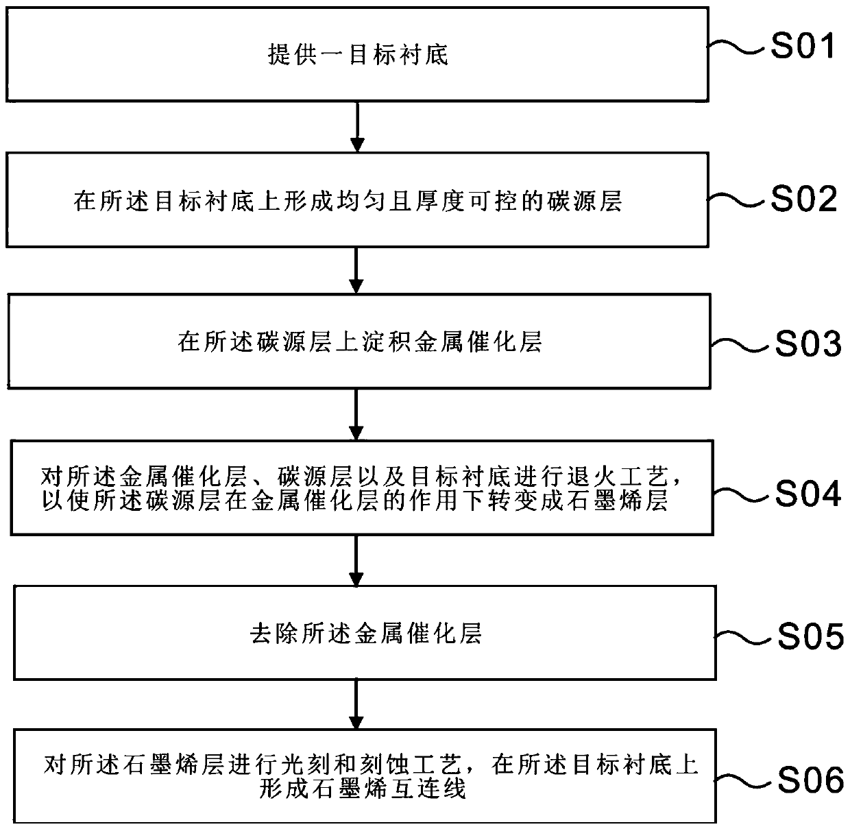
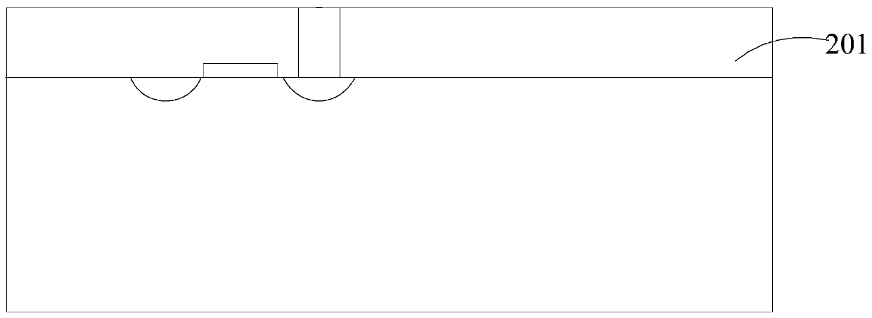
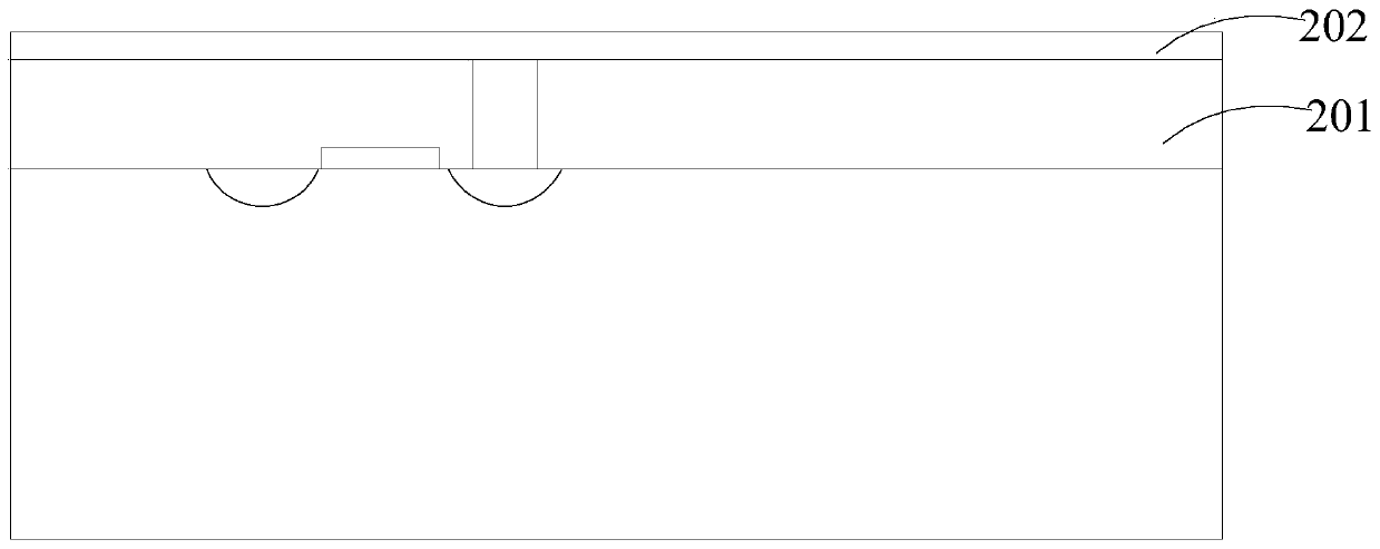
[0031] see figure 1 , figure 1 It is a schematic flow diagram of a preferred embodiment of a method for forming graphene interconnection provided by the present invention; at the same time, please refer to Figure 2a-2f , Figure 2a-2f It is a structural schematic diagram of a preferred embodiment for forming graphene interconnection provided by the present invention.
[0032] The present invention provides a method for forming graphene interconnection lines, comprising steps S01 to S06, specifically as follows:
[0033] Such as Figure 2a As shown, step S01: provide a target substrate 201; in this embodiment, the target substrate 201 has completed the preparation of transistor front-end process and via interconnection, and the target substrate 201 includes transistors fabricated on the substrate Included device layers and copper interconnect structures.
[0034] Such as Figure 2b As shown, step S02: forming a uniform and thickness-controllable carbon source layer 202 o...
Embodiment 2
[0040] In the second embodiment, a method for forming a metal / graphene hybrid interconnection line will be introduced. Please refer to Figure 3a-3f , Figure 3a-3f It is a structural schematic diagram of a preferred embodiment of a method for forming a metal / graphene hybrid interconnection provided by the present invention.
[0041] Different from Embodiment 1, in this embodiment, steps S03 and S05 in Embodiment 1 can be selectively skipped in the method for forming graphene interconnection lines, only steps S01, S02, S04 and S06, specifically Include the following steps:
[0042] Such as Figure 3a As shown in -c, step S01: provide a target substrate 301; specifically, the target substrate 301 has completed the preparation of transistor front-end process and via interconnection, and the target substrate includes transistors fabricated on the substrate. internal device layers and copper interconnect structures. In this embodiment, an intermetallic dielectric layer 302 can ...
PUM
| Property | Measurement | Unit |
|---|---|---|
| carrier mobility | aaaaa | aaaaa |
Abstract
Description
Claims
Application Information


