Method used for manufacturing multi-layer circuit board by employing 3D printing technology

A multi-layer circuit board, 3D printing technology, applied in the direction of printed circuit, printed circuit manufacturing, electrical components, etc., can solve the problems of high missed inspection rate, unrealizable, high labor intensity, etc., and achieve small equipment investment, less defect, low cost effect

Inactive Publication Date: 2015-04-01
ANHUI NEOFOUND TECH +2
View PDF4 Cites 26 Cited by
  • Summary
  • Abstract
  • Description
  • Claims
  • Application Information

AI Technical Summary

Problems solved by technology

Because the automatic detection system of printed circuit boards in foreign countries is too expensive, and the automatic detection equipment of printed circuit boards in the true sense has not been developed in China, most domestic circuit board manufacturers still use manual inspection with a magnifying glass or a projector. check side
Due to the high labor intensity of manual inspection, the eyes are prone to fatigue, and the missed inspection rate is high
Moreover, with the development of electronic products towards miniaturization and digitalization, printed circuit boards are also developing towards high density and high precision.
For higher density and precision circuit boards (0.12~0.10mm), it is completely impossible to inspect
Due to the backwardness of detection methods, the qualified rate of domestic multi-layer boards (8-12 layers) is only 50-60%.

Method used


Image

  • Method used for manufacturing multi-layer circuit board by employing 3D printing technology

Examples


Embodiment Construction

[0015] In order to better illustrate the present invention and facilitate understanding of the technical solutions of the present invention, typical but non-limiting examples of the present invention are as follows.

[0016] Use protel DXP software to design a 3-layer circuit board, convert the circuit board design into Gerber data format, and then send it to the laser 3D printer.

[0017] The raw material of the heat-resistant insulating layer is alumina ceramic powder; the ratio of circuit raw material powder is 95% Cu alloy and 5% tin-lead alloy.

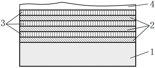
[0018] Using a laser 3D printer, the ceramic powder is molded using the selective laser sintering (SLS) method to form a heat-resistant insulating layer and protective layer, and the circuit is formed using the direct metal laser sintering (DMLS) method. So back and forth, and finally complete the printing.

[0019] The applicant declares that the above content is a further detailed description of the present invention in conj...


PUM


Abstract

The invention provides a method used for manufacturing a multi-layer circuit board by employing the 3D printing technology. The method is additionally provided with a heatproof insulation layer on the basis of an original printed circuit board. Raw material powder of the circuit comprises copper alloy powder and tin powder which are in a certain proportion, the heatproof insulation layer is ceramic powder, the 3D molding method is a laser irradiation molding method. During processing, the computer auxiliary manufacturing (CAM) technology is firstly utilized, circuit board design is accomplished on computer software and is transmitted to a 3D printer. The ceramic powder is fixed on the circuit board to form the heatproof insulation layer by utilizing the laser 3D printer, circuit molding of the powder is directly carried out on the heatproof insulation layer base body by utilizing the 3D printing technology, the steps above are repeated, and thereby the multi-layer circuit board is formed. Compared with a traditional printed circuit board, the multi-layer circuit board can be rapidly produced in a lab or under the small-batch production condition, moreover, the circuit does not easily generate defects, cost is low, response is rapid, equipment investment is small, and the method employing the 3D printing technology provides feasible small-batch customized production.

Description

Technical field: [0001] The invention relates to a method for manufacturing a multilayer circuit board by using 3D printing technology, which belongs to the technical field of electronic circuit processing. Background technique: [0002] 3D printing is a kind of rapid prototyping technology. It is a technology based on digital model files and using bondable materials such as powdered metal or plastic to construct objects by layer-by-layer printing. 3D printing is usually achieved using digital technology material printers. It is often used to make models in the fields of mold manufacturing and industrial design, and is gradually used in the direct manufacture of some products. There are already parts printed using this technology. The technology has applications in jewelry, footwear, industrial design, architecture, engineering and construction (AEC), automotive, aerospace, dental and medical industries, education, geographic information systems, civil engineering, firearm...

Claims


Application Information

Patent Timeline
Patent Type & Authority Applications(China)
IPC IPC(8): H05K3/12
CPCH05K3/12H05K3/4655H05K3/4664H05K2203/107
Inventor 聂刚谢峰龙海敏
Owner ANHUI NEOFOUND TECH
Why Eureka
Try Eureka