A kind of test method of dark current of long-wave hgcdte photovoltaic device
A test method and technology for photovoltaic devices, applied in the field of communication, can solve the problem that dark current cannot be measured quickly and accurately at low cost, and achieve the effects of convenient batch analysis, short time and low cost
- Summary
- Abstract
- Description
- Claims
- Application Information
AI Technical Summary
Problems solved by technology
Method used
Image
Examples
Embodiment 1
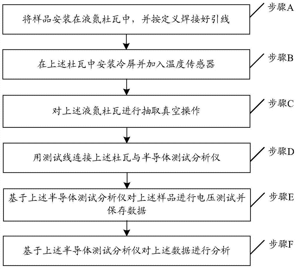
[0027] figure 1 It is a flow chart of a test method for dark current of a long-wave HgCdTe photovoltaic device according to Embodiment 1 of the present invention, such as figure 1 As shown, the method includes:
[0028] Step A, install the sample in a liquid nitrogen Dewar, and solder the leads as defined. Specifically, step A includes: sticking the sample on the cold head of Zhongce Dewar.
[0029] Step B, install a cold screen and add a temperature sensor in the above Dewar.
[0030] Step C, performing a vacuum extraction operation on the above-mentioned cold screen. Specifically, step C includes: performing a vacuum extraction operation on the liquid nitrogen Dewar until the vacuum degree reaches 1 torr.
[0031] Step D, connect the above-mentioned Dewar to the semiconductor test analyzer with a test line.
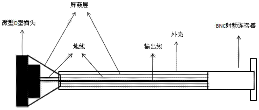
[0032] One end of the above-mentioned test line is a BNC RF connector, the other end is a miniature D-type plug, and the middle is set as an RF cable. The above-me...
Embodiment 2
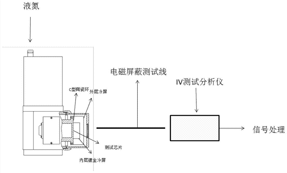
[0048] figure 2 It is a schematic diagram of the dark current test structure according to Embodiment 2 of the present invention, such as figure 2 As shown, the embodiment of the present invention first uses the test die of the chip as the sample material, so that the measurement can be carried out on the pn junction itself, which is a non-destructive measurement in itself, and avoids the interference of external factors such as the introduction of circuits.
[0049] In addition, in order to reduce the radiation noise of the background, the previous single-layer sealed cold shield was changed to a structure composed of a c-ring (rc ceramic ring), an inner cold shield, and an outer cold shield. The inner cold screen is supported on the top, and the vacuum in the middle of the double-layer cold screen can better reduce the heat exchange between the background of the detector and the outside world, making the background temperature lower. In addition, the inner cold screen is go...
Embodiment 3
[0055] The test method for the dark current of the long-wave HgCdTe photovoltaic device in this embodiment is as follows: firstly, the sample is pasted on the cold head of the Zhongce Dewar, and welded according to the definition, and then a c-shaped ring is placed around the sample, and on the c-shaped ring Paste the inner gold-plated cold screen, and evenly fill the thermal grease on the c-shaped ceramic ring, then add a temperature sensor on the outer surface of the inner cold screen, then install the outer cold screen, and finally buckle the window seat on the outside, and then start pumping Vacuum, stop when the vacuum reaches 1torr, then pour liquid nitrogen into the test Dewar, and monitor the temperature of the inner cold screen in real time, when the sensor value is stable at around 1.05 (80k), connect the Dewar to the semiconductor analyzer , carry out the IV test of the sample, the test result is as follows Figure 4 As shown, the data signal is finally processed fo...
PUM
 Abstract
Description
Claims
Application Information


