

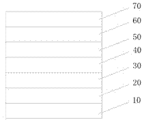
Indium nitride channel layer gallium nitride-based high-electron-mobility transistor structure
A high electron mobility, indium nitride channel technology, applied in circuits, electrical components, semiconductor devices, etc., can solve the problem that the p-type doping technology of the gallium nitride buffer layer is difficult to achieve, reduce the material lattice integrity, The crystal quality of the buffer layer is degraded, and the effect of improving the confinement ability of the two-dimensional electron gas, suppressing the short channel effect, and improving the confinement ability is achieved.
- Summary
- Abstract
- Description
- Claims
- Application Information
AI Technical Summary
Problems solved by technology
Method used
Image

Examples
Embodiment Construction
[0026] The present invention will now be described more fully with reference to the accompanying drawings, in which exemplary embodiments of the invention are shown. This invention may, however, be embodied in many different forms and should not be construed as limited to the exemplary embodiments set forth herein. Rather, these embodiments are provided so that this disclosure will be thorough and complete, and will fully convey the scope of the invention to those skilled in the art.
[0027] For ease of description, spatially relative terms such as "upper," "lower," "left," and "right" may be used herein to describe the relationship of one element or feature relative to another element or feature shown in the figures. It will be understood that the spatial terms are intended to encompass different orientations of the device in use or operation in addition to the orientation depicted in the figures. For example, if the device in the figures is turned over, elements described ...
PUM
| Property | Measurement | Unit |
|---|---|---|
| Thickness | aaaaa | aaaaa |
| Thickness | aaaaa | aaaaa |
| Thickness | aaaaa | aaaaa |
Abstract
Description
Claims
Application Information