Preparation method for inverted pyramid structure on silicon wafer surface
A silicon chip surface and inverted pyramid technology, applied in semiconductor/solid-state device manufacturing, electrical components, circuits, etc., to achieve low cost, easy promotion and application, and reduce production costs
- Summary
- Abstract
- Description
- Claims
- Application Information
AI Technical Summary
Problems solved by technology
Method used
Image
Examples
preparation example Construction
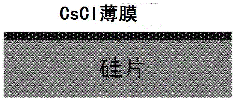
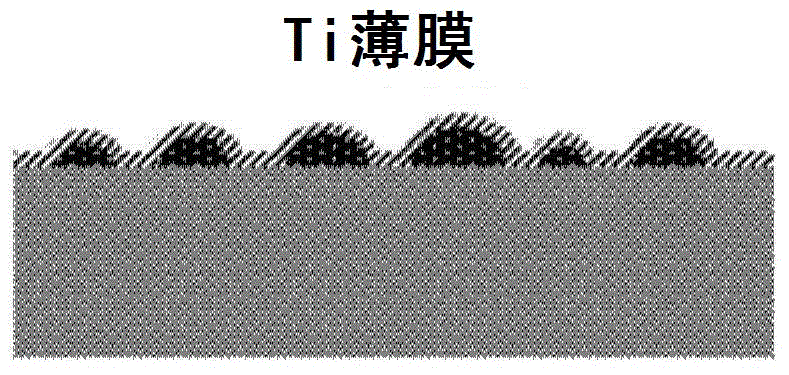
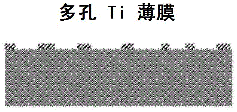
[0031] based on figure 1 The preparation method of the silicon wafer surface inverted pyramid structure shown, Figure 2-Figure 7 Shown is the process flow chart of preparing the inverted pyramid structure on the surface of silicon wafer according to the embodiment of the present invention. The preparation of face inverted pyramid specifically comprises the following steps:
[0032] Such as figure 2 As shown, the silicon wafer is cleaned and placed in a vacuum coating chamber to evaporate a cesium chloride film with a film thickness of 200-7000 angstroms; the silicon wafer is a silicon wafer used in the semiconductor industry with a thickness of 0.2mm-0.5mm, P-type , the resistivity is 1Ω·cm-10Ω·cm, and the surface is polished.
[0033] Such as image 3 As shown, after the cesium chloride thin film is plated, the gas with a certain humidity is introduced into the vacuum coating cavity, and the relative humidity is 10%-70%. Nano-cesium chloride peninsula structures simila...
Embodiment
[0040] The following is a process flow chart for preparing an inverted pyramid structure on the surface of a silicon wafer according to an embodiment of the present invention. The method includes the following steps:
[0041] Step 1: Evaporate a cesium chloride film on a silicon wafer by thermal evaporation, the film thickness is 300 nanometers, and the thickness is measured and controlled by a quartz crystal thickness gauge.
[0042] Step 2: Put the silicon wafer coated with a cesium chloride film into a ventilated chamber with a humidity of 50%, the humidity is controlled by the flow of humid gas flowing into the chamber, develop for 1 hour under this humidity condition, and make the cesium chloride The thin film is aggregated into a nano-island structure, and a cesium chloride nano-island structure is formed on the surface of the silicon wafer; the average diameter of the cesium chloride nano-island is 600 nanometers.
[0043] Step 3: Put the silicon wafer with the cesium c...
PUM
| Property | Measurement | Unit |
|---|---|---|
| Thickness | aaaaa | aaaaa |
| Resistivity | aaaaa | aaaaa |
| Diameter | aaaaa | aaaaa |
Abstract
Description
Claims
Application Information


