

Perovskite solar cell and manufacturing method thereof
A solar cell and perovskite technology, applied in the field of solar cells, can solve problems such as the influence of solar cell product quality and pass rate, damage to the perovskite layer and hole transport layer, and poor contact, so as to facilitate charge exchange and avoid Poor contact or short circuit, the effect of reducing internal resistance
- Summary
- Abstract
- Description
- Claims
- Application Information
AI Technical Summary
Problems solved by technology
Method used
Image

Examples
Embodiment 1
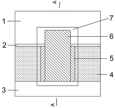
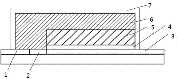
[0029] see figure 1 and figure 2 , first, use an infrared laser (wavelength 1064 nanometers) to etch an insulating band 2 parallel to the side at a distance of 0.8 cm from the edge of one side on the conductive layer of FTO conductive glass with a size of 2.0 cm × 2.0 cm. The width of the insulating band 2 is 0.05 cm, divide the conductive glass into the positive electrode area 1 (0.8 cm × 2.0 cm in size) and the negative electrode area 3 (1.2 cm × 2.0 cm in size), so that the conductive layer cannot be completely conducted, and the conductive glass after etching is sequentially washed Ultrasonic cleaning with solvent, distilled water and absolute ethanol.
[0030] Then, a titanium tetrachloride solution with a mass concentration of 0.05% was sprayed on the surface of the negative electrode region 3 of the conductive glass at a temperature of 450°C to form a dense barrier layer 4 with a thickness of 22 nanometers.
[0031] Take 8g of zirconium dioxide powder with a particle...
Embodiment 2
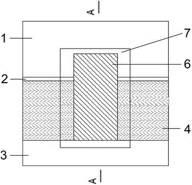
[0035] see image 3 and figure 2 First use an infrared laser with a wavelength of 1064 nanometers to etch an insulating band 2 parallel to the side at a distance of 1.1 cm from the edge of one side of the conductive layer of FTO conductive glass with a size of 3.0 cm × 3.0 cm. The width of the insulating band 2 is 0.05 cm. , divide the conductive glass into positive electrode area 1 (1.1 cm × 3.0 cm in size) and negative electrode area 3 (1.9 cm × 3.0 cm in size), so that the conductive layer cannot be completely conducted, and the conductive glass after etching is sequentially used with detergent , distilled water and ethanol for ultrasonic cleaning.
[0036] Then spray a titanium tetrachloride solution with a mass concentration of 0.1% on the surface of the negative electrode region 3 of the conductive glass at a temperature of 400 oC to form a dense barrier layer 4 with a thickness of 28 nanometers.
[0037]Take 8g of zirconia powder with a particle size of 80 nanometers...
PUM
| Property | Measurement | Unit |
|---|---|---|
| Particle size | aaaaa | aaaaa |
Abstract
Description
Claims
Application Information