
Positive photoresist-based nickel positive mold production method

A technology of positive photoresist and photoresist, which is applied in the direction of microlithography exposure equipment, photosensitive material processing, photolithography process exposure device, etc., which can solve the problem of edge warping, difficult deglue process, and low photolithography preparation efficiency And other issues

Active Publication Date: 2015-05-06
北京同方光盘股份有限公司
View PDF5 Cites 4 Cited by
  • Summary
  • Abstract
  • Description
  • Claims
  • Application Information

AI Technical Summary

Problems solved by technology

[0004] The embodiment of the present invention provides a method for making a positive photoresist-based nickel positive mold, which solves the problems of low photolithography preparation efficiency, difficult desmearing process, and edge warping

Method used


Image

  • Positive photoresist-based nickel positive mold production method
  • Positive photoresist-based nickel positive mold production method
  • Positive photoresist-based nickel positive mold production method

Examples


Embodiment Construction

[0025] In order to make the object, technical solution and advantages of the present invention clearer, the specific embodiments of the present invention will be further described in detail below in conjunction with the accompanying drawings.

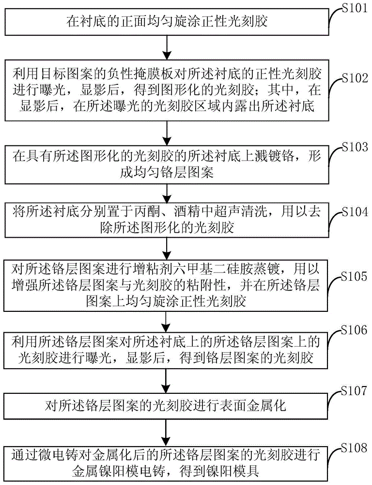
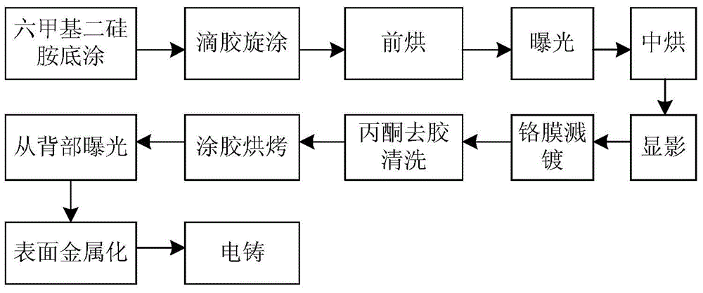
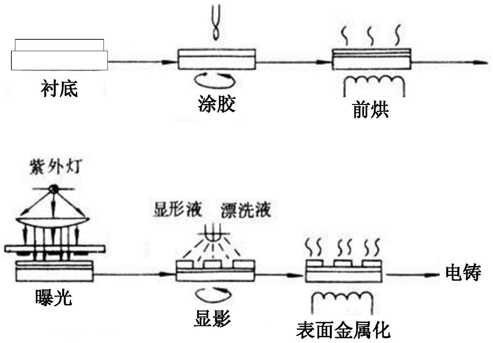
[0026] Below to figure 1 As an example to describe in detail the positive photoresist-based nickel positive mold manufacturing method provided by the embodiment of the present invention, figure 1 The flow chart of the positive photoresist-based nickel positive mold manufacturing method provided by the embodiment of the present invention; figure 2 The schematic flow chart of the positive photoresist-based nickel positive mold manufacturing method provided by the embodiment of the present invention; image 3 A schematic diagram of the production scene of a positive photoresist-based nickel positive mold provided by the embodiment of the present invention. Such as figure 1 , 2 As shown in and 3, the method includes the following steps...


PUM

PropertyMeasurementUnit
Draft angleaaaaaaaaaa

Abstract

The embodiment of the invention relates to a positive photoresist-based nickel positive mold production method. The method comprises the following steps: evenly spin-coating the front side of a substrate with a positive photoresist; exposing the positive photoresist of the substrate by utilizing a negative mask plate of a target pattern, and developing to obtain the patterned photoresist; splash-plating chromium on the substrate with the patterned photoresist, to form a uniform chromium layer pattern; performing tackifier hexamethyldisilazane evaporation on the chromium layer pattern so as to enhance the adhesiveness of the chromium layer pattern and the photoresist, and evenly spin-coating the chromium layer pattern with the positive photoresist; exposing the photoresist on the chromium layer pattern on the substrate by utilizing the chromium layer pattern, and developing to obtain the photoresist of the chromium layer pattern; performing surface metallization on the photoresist of the chromium layer pattern; and performing metal nickel positive mold electroforming on the photoresist of the metalized the chromium layer pattern, to obtain the nickel positive mold. For the nickel positive mold, the production technology is simple and convenient, the photoresist removal is convenient, and the upwarping edges of the nickel positive mold can be avoided.

Description

technical field [0001] The invention relates to the field of microfluidic chip preparation, in particular to a method for manufacturing a positive photoresist-based nickel positive mold. Background technique [0002] Lithography technology is widely used in the field of microfluidic chip preparation. The quality of lithography directly affects the quality of the metal positive mold and its microfluidic chip. Optimizing and adjusting the lithography process and methods is crucial to improving product quality. role. Therefore, optimizing and adjusting the photolithography process is particularly important for the precise and rapid preparation of microfluidic chips. Due to the existence of light diffraction and other phenomena in thick photoresist lithography technology, the angle α between the photoresist pattern and the substrate is not equal to 90°. If the angle α between the photoresist pattern and the substrate is not greater than 90°, the photoresist The side wall of th...

Claims


Application Information

Patent Timeline
IPC IPC(8): G03F7/20G03F7/42
Inventor 郭哲刘祝凯宋娇阳许斌
Owner 北京同方光盘股份有限公司
Learn More