Preparation method for ultrathin up-right graphene field emission cathode rich in wrinkle on surface

A technology that emits cathodes and graphene, applied in cold cathode manufacturing, electrode system manufacturing, discharge tube/lamp manufacturing, etc., can solve problems such as increasing graphene surface, reducing turn-on and threshold fields, and large gaps

Inactive Publication Date: 2015-05-13
TIANJIN NORMAL UNIVERSITY
View PDF2 Cites 15 Cited by
  • Summary
  • Abstract
  • Description
  • Claims
  • Application Information

AI Technical Summary

Problems solved by technology

However, the thickness of these upright graphene is often more than 10 layers and the surface is flat, and the open field of the field emission cathode material is generally above 4 V / μm, which is different from carbon nanotubes, a traditional excellent field emission cathode material. There is still a big gap compared to (the turn-on field of carbon nanotubes is generally 1-2V / μm)
[0005] According to the existing theoretical research surface, increasing the wrinkles and defects on the graphene surface can increase the number of its effective field emission points, increase its field enhancement factor, thereby reducing its turn-on and threshold fields

Method used


Image

  • Preparation method for ultrathin up-right graphene field emission cathode rich in wrinkle on surface
  • Preparation method for ultrathin up-right graphene field emission cathode rich in wrinkle on surface
  • Preparation method for ultrathin up-right graphene field emission cathode rich in wrinkle on surface

Examples


Embodiment 1

[0033] (1) Preparation of silicon substrate:

[0034] First cut the silicon wafer into small pieces of 2cm×2cm, ultrasonically clean it in acetone, absolute ethanol, and deionized water for about 10 minutes, and the ultrasonic power is 50W, and then immerse the silicon wafer in hydrofluoric acid with a volume ratio of 4% for 5 minutes. In minutes, a silicon wafer substrate that is clean, pollution-free and free of surface oxide is obtained.

[0035] (2) Growing upright graphene:

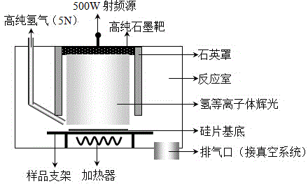
[0036] The growth of vertical graphene is completed in a radio frequency sputtering device, and the schematic diagram of the device is shown in figure 1 shown. Place the prepared silicon substrate on the sample stage in the reaction chamber, and evacuate the reaction chamber to about 8 × 10 -4 Pa; then pass high-purity hydrogen (5N) into the reaction chamber, adjust the pressure of the reaction chamber to 300Pa; heat the substrate to 1100K at a speed of about 60K / min; after the temperature and pre...

Embodiment 2

[0042] (1) Preparation of silicon substrate:

[0043] First cut the silicon wafer into small pieces of 2cm×2cm, ultrasonically clean it in acetone, absolute ethanol, and deionized water for about 10 minutes, and the ultrasonic power is 50W, and then immerse the silicon wafer in hydrofluoric acid with a volume ratio of 4% for 5 minutes. In minutes, a silicon wafer substrate that is clean, pollution-free and free of surface oxide is obtained.

[0044] (2) Growing upright graphene:

[0045] The growth of vertical graphene is completed in a radio frequency sputtering device, and the schematic diagram of the device is shown in figure 1 shown. Place the prepared silicon substrate on the sample stage in the reaction chamber, and evacuate the reaction chamber to about 8 × 10 -4 Pa; then pass high-purity hydrogen (5N) into the reaction chamber, adjust the pressure of the reaction chamber to 280Pa; heat the substrate to 1100K at a speed of about 60K / min; after the temperature and pre...

Embodiment 3

[0051] (1) Preparation of silicon substrate:

[0052] First cut the silicon wafer into small pieces of 2cm×2cm, ultrasonically clean it in acetone, absolute ethanol, and deionized water for about 10 minutes, and the ultrasonic power is 50W, and then immerse the silicon wafer in hydrofluoric acid with a volume ratio of 4% for 5 minutes. In minutes, a silicon wafer substrate that is clean, pollution-free and free of surface oxide is obtained.

[0053] (2) Growing upright graphene:

[0054] The growth of vertical graphene is completed in a radio frequency sputtering device (commercially available), and the schematic diagram of the device is shown in figure 1 shown. Place the prepared silicon substrate on the sample stage in the reaction chamber, and evacuate the reaction chamber to about 8 × 10 -4 Pa; then pass high-purity hydrogen (5N) into the reaction chamber, adjust the pressure of the reaction chamber to 320Pa; heat the substrate to 1100K at a speed of about 60K / min; afte...


PUM

PropertyMeasurementUnit
current densityaaaaaaaaaa
thicknessaaaaaaaaaa
lengthaaaaaaaaaa

Abstract

The invention discloses a preparation method for ultrathin up-right graphene field emission cathode rich in wrinkle on surface and belongs to the preparation and application field of the nanometer material. The preparation method mainly comprises the following preparation technology: taking the monocrystalline silicon piece or metal piece with flat surface or carbon nanotube array or silicon nanowire array having nano structure on surface as the substrate; adopting the radio frequency sputtering for growing the ultrathin up-right graphene rich in wrinkle on surface without catalytic on the substrate; and taking the obtained ultrathin up-right graphene rich in wrinkle on surface as the cathode for assembling the field electronic emitter. The up-right graphene is very thin, the average layer number is five, much wrinkle is formed on the surface with defect, the surface of up-right graphene is flat and the up-right grapheme has lower opening field, threshold value field, good field emission stability and higher application value.

Description

[0001] This invention is funded by the National Natural Science Foundation of China-Youth Fund Project (Project No. 51302187); by the Key Project of Tianjin Applied Basic and Frontier Technology Research Program (Project No. 14JCZDJC32100). technical field [0002] The invention belongs to the technical field of preparation and application of nanometer materials, and relates to a method for preparing a new nanometer material with a unique structure by using plasma technology and using it for field electron emission devices. Background technique [0003] The development of high-performance field emission materials is currently a research hotspot. Its application fields involve X light sources, new generation vacuum tubes, high-current electron sources of electron accelerators, electron guns of field emission electron microscopes, cold cathode field emission flat panel displays and many other aspects. Graphene, as a new type of carbon nanomaterial, has become an ideal field emi...

Claims


Application Information

Patent Timeline
Patent Type & Authority Applications(China)
IPC IPC(8): H01J1/304H01J9/02
CPCH01J1/304H01J1/3048H01J9/025
Inventor 邓建华程国安汪凡洁
Owner TIANJIN NORMAL UNIVERSITY
Why Eureka
Try Eureka