Near infrared LED and production method thereof

A technology for light-emitting diodes and production methods, applied in electrical components, circuits, semiconductor devices, etc., can solve the problems of low thermal resistance, low reflectivity of oblique incident light, complicated processes, etc., achieve high transmittance, simplify the process, Avoid the effect of substrate shading

Active Publication Date: 2015-05-13
YANGZHOU CHANGELIGHT
View PDF6 Cites 23 Cited by
  • Summary
  • Abstract
  • Description
  • Claims
  • Application Information

AI Technical Summary

Problems solved by technology

[0003] Traditional high-brightness AlGaAs near-infrared light-emitting diodes mainly use metal bonding technology to realize substrate replacement, and use silicon substrates with better thermal conductivity (the thermal conductivity of silicon is about 1.5W/K.cm) to replace gallium arsenide linings. bottom (the thermal conductivity of gallium arsenide is about 0.8W/K.cm), the chip has lower thermal resistance and better heat dissipation performance, but because the silicon substrate is opaque and still has the prob

Method used


Image

  • Near infrared LED and production method thereof
  • Near infrared LED and production method thereof

Examples


Embodiment Construction

[0025] 1. Manufacturing steps:

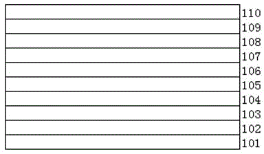
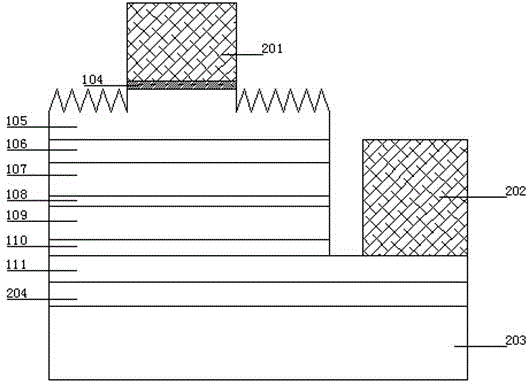
[0026] 1. If figure 1 As shown, make N-GaAs epitaxial wafer:

[0027] 1) Using MOCVD equipment to sequentially grow N-GaAs buffer layer 102, N-GaInP cut-off layer 103, N-GaAs ohmic contact layer 104, N-AlGaAs roughening layer 105, N- AlGaAs current spreading layer 106 , N-AlGaAs confinement layer 107 , MQW multiple quantum well active layer 108 , P-AlGaAs confinement layer 109 , P-AlGaAs current spread layer 110 .

[0028] Wherein the N-GaAs ohmic contact layer 104 preferably has a thickness of 50nm and a doping concentration of 1×10 19 cm -3 , the doped impurity element is silicon (Si), to ensure that the first electrode has good electrical contact with the N surface; the preferred thickness of the P-AlGaAs current spreading layer 110 is 4000nm, and the doping concentration is 7×10 18 cm -3 , the doped impurity element is magnesium (Mg) to ensure good ohmic contact and current spreading ability on the P surface; the Al component in the N-...


PUM

PropertyMeasurementUnit
Thicknessaaaaaaaaaa
Thicknessaaaaaaaaaa
Thicknessaaaaaaaaaa

Abstract

The invention provides a near infrared LED and a production method thereof, and belongs to the technical field of photoelectron. The method comprises the steps of forming an epitaxial wafer on a temporary substrate; manufacturing a transparent conductive layer on a current expansion layer of the epitaxial wafer; annealing to enable the transmission rate and square resistance of the transparent conductive layer; enabling the transparent conductive layer to be opposite to a transparent permanent substrate; integrally adhering the epitaxial wafer and the transparent permanent substrate through adhesive; removing the temporary substrate, a N-GaAs buffer layer and a N-GaInP stop layer; exposing an N-GaAs ohm contact layer; corroding to form a pattern; roughing; manufacturing a first electrode on the patterned N-GaAs area; annealing to electrically connect the first electrode and the N-GaAs. With the adoption of the method, the transmission rate of the near infrared wave section is high, and the light outgoing efficiency is further increased; the parallel structures of the electrodes at the P side and the N side can be achieved; the transparent conductive layer is also an anti-reflection film which increases the light picking efficiency.

Description

technical field [0001] The invention belongs to the technical field of optoelectronics, in particular to the technical field of manufacturing AlGaAs ternary system near-infrared light-emitting diodes. Background technique [0002] Infrared light-emitting diodes are widely used in remote control, medical equipment, space communication, infrared lighting and other fields due to their specific wavelength band, low power consumption and high reliability. [0003] Traditional high-brightness AlGaAs near-infrared light-emitting diodes mainly use metal bonding technology to realize substrate replacement, and use silicon substrates with better thermal conductivity (the thermal conductivity of silicon is about 1.5W / K.cm) to replace gallium arsenide linings. bottom (the thermal conductivity of gallium arsenide is about 0.8W / K.cm), the chip has lower thermal resistance and better heat dissipation performance, but because the silicon substrate is opaque and still has the problem of ...

Claims


Application Information

Patent Timeline
IPC IPC(8): H01L33/00H01L33/42H01L33/02H01L33/44H01L33/22
CPCH01L33/0062H01L33/0093H01L33/22H01L33/42H01L2933/0016
Inventor 白继锋陈凯轩杨凯林志伟李俊承陈宝张双翔张银桥王向武
Owner YANGZHOU CHANGELIGHT
Why Eureka
Try Eureka