
Random access memory with redundant structure

A technology of random access and redundant structure, which is applied in the direction of static memory, digital memory information, information storage, etc., can solve the problems of high process cost, difficult integration, low speed, etc., and achieve good process compatibility, small unit area, and design simple effect

Active Publication Date: 2015-05-20
TSINGHUA UNIV +1
View PDF4 Cites 3 Cited by
  • Summary
  • Abstract
  • Description
  • Claims
  • Application Information

AI Technical Summary

Problems solved by technology

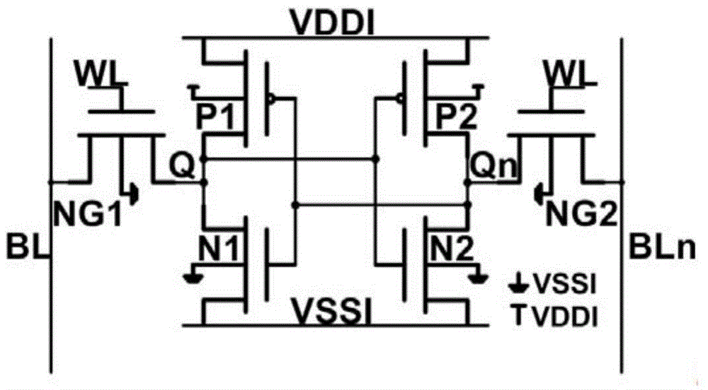
Due to the need to increase the resistance process, the speed is low, the integration is difficult, and the reinforcement capability is difficult to guarantee in harsh environments, the resistance reinforcement is greatly limited in application; process reinforcement methods (such as SOI process, epitaxial process, etc.) The amount of charge collected can effectively improve the ability of the memory cell to resist single event flipping, but its biggest disadvantage is that the process cost is high, and it is not compatible with the existing mainstream CMOS process; the system error correction and reinforcement technology can be solved from the peripheral circuit level The error caused by the single event effect of the SRAM unit ensures the correctness of the system. However, as the line width of the process shrinks to the nanometer scale, the area of ​​the SRAM unit continues to shrink, and the error rate rises sharply, resulting in an increase in the cost of the error correction circuit. Refresh frequency increases, memory speed performance degrades; circuit design reinforcement generally uses two ideas of "redundancy" and "recovery" to design complex memory units, which can obtain good radiation resistance. The existing common memory unit structures include: 6T2C , 6T2C2R, 8T, 10T, 12T, DICE, etc.
However, the external circuit design of the traditional circuit design reinforcement method is relatively complicated, and the size of the memory cell is large, so it is not widely used in the process node above 0.18 microns

Method used


Image

  • Random access memory with redundant structure
  • Random access memory with redundant structure
  • Random access memory with redundant structure

Examples


Embodiment Construction

[0021] In order to make those skilled in the art understand better, the applicant makes a brief introduction to the prior art and its shortcomings. At this stage, the more commonly used reinforcement technology is the three-mode redundancy reinforcement technology, which belongs to the circuit design reinforcement technology. But strictly speaking, Triple Modular Redundancy (TMR) is an architecture-level reinforcement. The mechanism of its anti-SEU is as follows figure 2 shown. Its design idea is: add two redundant memory units, then send the output of the three memories to the majority voting circuit, and the result after voting is the final output result. The working truth table of the majority voting circuit is shown in the table. It can be seen from Table 1 that if the data in one of the three memories is flipped, the wrong data can be masked out after voting through the voting circuit.

[0022] Table 1 TMR hardened voting circuit truth table

[0023] SRAM0 ...


PUM


Abstract

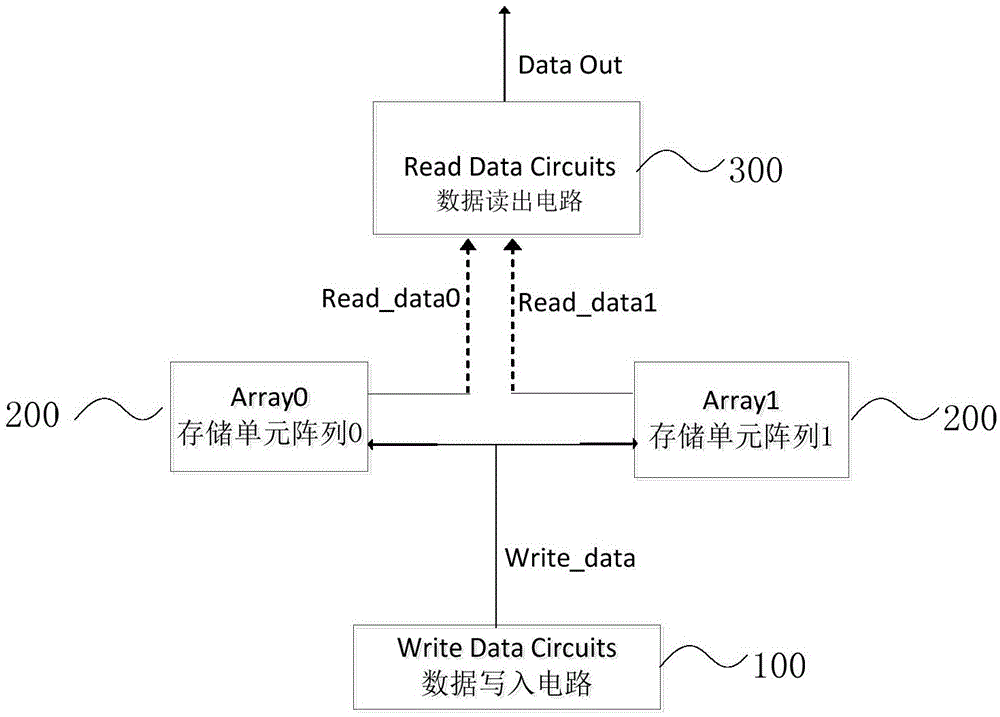
The invention discloses a random access memory with a redundant structure. The random access memory comprises two same memory unit arrays, a data writing circuit and a data reading circuit, wherein the two same memory unit arrays have same array frameworks; memory units at the same address in the arrays have the same initial memory information; the data writing circuit is used for simultaneously writing the same data into the memory units at the same addresses in the two same memory arrays; and the data reading circuit is used for selecting memory information in the memory units at the same addresses in the two memory unit arrays, outputting 0 when the memory information in the two memory units is not different and outputting the same memory information when the memory information in the two memory units is the same. The random access memory has the advantages of small hardware area, low complexity, stable and reliable data storage and the like.

Description

technical field [0001] The invention belongs to the technical field of memory design, and in particular relates to a redundant structure random access memory. Background technique [0002] With the development of nuclear energy technology and space technology, more and more electronic devices need to be used in various radiation environments. With the improvement of system performance requirements for space applications, the reduction of device feature size and the advancement of technology, the sensitivity of semiconductor devices to space radiation increases, and the influence of single event effects (Single Event Effect, SEE) is rapidly expanding. Static Random Access Memory (SRAM) is widely used in various military and space systems. However, the bistable circuit structure of the SRAM unit is particularly sensitive to the single event upset effect, which will cause errors in stored data and disordered instruction programs. In severe cases, it will cause the failure of t...

Claims


Application Information

Patent Timeline
IPC IPC(8): G11C11/413
CPCG11C11/419G11C11/403G11C11/406G11C11/412G11C11/4125G11C11/418
Inventor 潘立阳洪新红伍冬
Owner TSINGHUA UNIV
Learn More