Organic electroluminescence device and preparation method thereof
An electroluminescent device and electroluminescent technology, which are applied in the fields of electro-solid devices, semiconductor/solid-state device manufacturing, electrical components, etc., can solve the problems of total reflection loss, low light output performance, refractive index difference, etc. Improve luminous efficiency and luminous color stability
- Summary
- Abstract
- Description
- Claims
- Application Information
AI Technical Summary
Problems solved by technology
Method used
Image

Examples
preparation example Construction
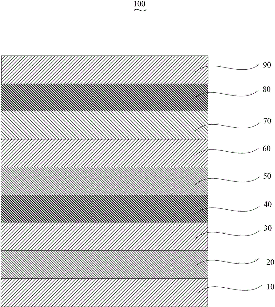
[0036] The preparation method of the organic electroluminescence device 100 of an embodiment, it comprises the following steps:
[0037] Step S110 , preparing the scattering layer 20 on the surface of the glass substrate 10 by electron beam evaporation.
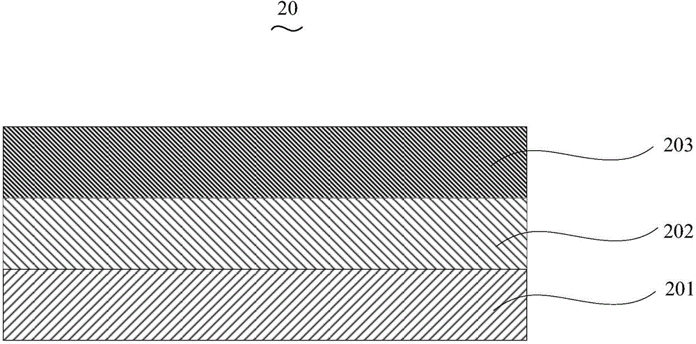
[0038] The scattering layer 20 is formed on one side surface of the glass substrate 10 . The scattering layer 20 is composed of a metal material layer 201 , a luminescent material doped layer 202 and a metal oxide doped layer 203 . A metal material layer is prepared on the surface of the glass substrate by thermal resistance evaporation, and the work function of the material of the metal material layer is -4.0~-5.5eV, and the luminescence is prepared on the surface of the metal material layer 201 by electron beam evaporation. A material doped layer 202, the luminescent material doped layer 202 includes a luminescent material and the first metal oxide material doped in the luminescent material, and the material of the lumines...
Embodiment 1
[0057] The structure prepared in this example is glass substrate / Ag / Alq 3 :ZrO 2 / MoO 3 :Alq 3 / ITO / MoO 3 / NPB / Alq 3 / TAZ / CsF / Ag organic electroluminescent device, in this embodiment and the following embodiments, " / " indicates a layer, and ":" indicates doping.
[0058] The glass substrate is N-LASF44. After rinsing the glass substrate with distilled water and ethanol, soak it in isopropanol for one night. Prepare a scattering layer on a glass substrate. The scattering layer is composed of a metal material layer, a luminescent material doped layer and a metal oxide doped layer. The metal material layer is prepared by thermal resistance evaporation on the surface of the glass substrate. The material is Ag and the thickness is 10nm. , on the surface of the metal material layer, the luminescent material doped layer is prepared by thermal resistance evaporation, and the material is Alq 3 :ZrO 2 , Alq 3 with ZrO 2 The mass ratio is 1.5:0.1, the thickness is 70nm, and the ...
Embodiment 2
[0066] The structure prepared in this example is glass substrate / Al / DCJTB:MgO / WO 3 :AND / IZO / V 2 o 5 / TCTA / ADN / Bphen / CsN 3 / Al organic electroluminescent devices.
[0067] The glass substrate is N-LAF36. After rinsing the glass substrate with distilled water and ethanol, soak it in isopropanol for one night to prepare a scattering layer on the glass substrate. The scattering layer consists of a metal material layer, a luminescent material doped layer and a metal oxide layer. The metal material layer is prepared by thermal resistance evaporation on the surface of the glass substrate, the material is Al, and the thickness is 5nm, and the luminescent material doped layer is prepared by thermal resistance evaporation on the surface of the metal material layer, and the material is DCJTB:MgO , the mass ratio of DCJTB to MgO is 1:0.1, and the thickness is 50nm. The metal oxide doped layer is prepared by electron beam evaporation on the surface of the luminescent material doped laye...
PUM
| Property | Measurement | Unit |
|---|---|---|
| thickness | aaaaa | aaaaa |
| thickness | aaaaa | aaaaa |
| thickness | aaaaa | aaaaa |
Abstract
Description
Claims
Application Information
 - R&D
- Intellectual Property
- Life Sciences
- Materials
- Tech Scout
- Unparalleled Data Quality
- Higher Quality Content
- 60% Fewer Hallucinations
Browse by: Latest US Patents, China's latest patents, Technical Efficacy Thesaurus, Application Domain, Technology Topic, Popular Technical Reports.
© 2025 PatSnap. All rights reserved.Legal|Privacy policy|Modern Slavery Act Transparency Statement|Sitemap|About US| Contact US: help@patsnap.com