Gas barrier film and method for manufacturing gas barrier film

A gas barrier film and gas barrier technology, which are used in the manufacture of semiconductor/solid state devices, electrical components, and electric solid state devices, etc., to achieve the effect of suppressing the reduction of gas barrier properties and excellent crack resistance

Active Publication Date: 2015-06-24
KONICA MINOLTA INC
View PDF13 Cites 9 Cited by
  • Summary
  • Abstract
  • Description
  • Claims
  • Application Information

AI Technical Summary

Problems solved by technology

[0006] However, the above-mentioned vapor deposition technology is at most only 1 (g / m 2 24h) water vapor barrier property

Method used


Image

  • Gas barrier film and method for manufacturing gas barrier film
  • Gas barrier film and method for manufacturing gas barrier film
  • Gas barrier film and method for manufacturing gas barrier film

Examples


Embodiment 1

[0348] (Substrate)

[0349] As a substrate, a biaxially stretched polyethylene naphthalate film (PEN film, thickness: 100 μm, width: 350 mm, manufactured by Teijin DuPont Films Co., Ltd., trade name “TEONEX Q65FA”) was used.

[0350] (Production of gas barrier layer)

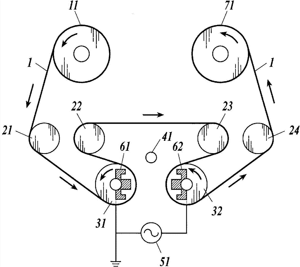
[0351] use figure 2 In the above-mentioned apparatus, the above-mentioned substrate was mounted on the apparatus, and a gas barrier layer was formed on the substrate to have a thickness of 300 nm under the following film-forming conditions (plasma CVD conditions). At this time, make the following samples: image 3 As shown, the gas supply port moves from the vertical bisector of the line segment between the electrodes of the film-forming roll to the side of the film-forming roll 31 or 32 as shown in Table 1 and moves parallel to the line segment between the electrodes of the film-forming roll by 2%, The distances of 5%, 10% and 20% increase the oxygen atomic ratio at the interface of the gas barrier layer on...

Embodiment 2

[0374] Such as Figure 8 As documented, connect the 2 and 3 above figure 2 The described apparatus is a tandem plasma CVD apparatus.

[0375] Using the above-mentioned device, the positions of the gas supply ports during the preparation of Sample Nos. 1-1, 1-2, 1-3, and 1-4 of Example 1 were set in the same manner, and the gas barriers of Example 1 were prepared. Under the same conditions, CVD was repeated 2 and 3 times to fabricate gas barrier film samples with a gas barrier layer thickness of 600 nm and 900 nm.

[0376]The same as in Example 1, the XPS depth profile was measured for the sample obtained, and the silicon distribution curve, oxygen distribution curve and carbon distribution curve were obtained. As a result, the samples No.2-1, No.2-2, and No. .3-1 and No.3-2's silicon atomic ratio, oxygen atomic ratio and carbon atomic ratio meet the requirements of (i) above; the obtained carbon distribution curve has multiple definite extreme values; the maximum value of t...

Embodiment 3

[0381] (Substrate)

[0382] As a substrate, a biaxially stretched polyethylene naphthalate film (PEN film, thickness: 100 μm, width: 350 mm, manufactured by Teijin DuPont Films Co., Ltd., trade name “TEONEX Q65FA”) was used.

[0383] (making of base layer)

[0384] After coating the easy-adhesive surface of the above substrate with a wire bar so that the layer thickness after drying is 4 μm, OPSTAR Z7501, a UV-curable organic / inorganic composite hard coating material manufactured by JSR Corporation, was dried under 80°C, 3 After drying for 10 minutes, in the air environment, use a high-pressure mercury lamp, according to the curing condition 1.0J / cm 2 Curing is carried out to form a base layer. The maximum profile height Rt(p) of the roughness curve representing the surface roughness at this time was 16 nm. It should be noted that the roughness curve is calculated using an AFM (atomic force microscope AFM: manufactured by Digital Instruments) using a probe with a stylus hav...


PUM

PropertyMeasurementUnit
thicknessaaaaaaaaaa
thicknessaaaaaaaaaa
particle sizeaaaaaaaaaa

Abstract

The present invention addresses the problem of providing a gas barrier film, which: has ample gas barrier properties even in a high temperature, high humidity use environment; adequately limits the decrease in gas barrier properties even when the film is bent; and also has excellent resistance to cracking. This gas barrier film is characterized in having a gas barrier layer containing silicon, oxygen and carbon on at least one surface of a base material and in satisfying all of the conditions (i) - (iv). (i) In a region extending to 90% or more of the layer thickness direction, the silicon, oxygen and carbon atomic ratios are (carbon atomic ratio ) < (silicon atomic ratio) < (oxygen atomic ratio), (ii) the carbon distribution curve has at least two extremes, (iii) the absolute value of the difference between the maximum value and the minimum value of the carbon atomic ratio in the carbon distribution curve is 5 at% or more, and (iv) the maximum of the oxygen distribution curve closest to the surface of the gas barrier layer on the base material side is the maximum value among the maxima of the oxygen distribution curve in said gas barrier layer.

Description

technical field [0001] The present invention relates to a gas barrier film and a method for producing the gas barrier film. More specifically, it relates to a transparent gas barrier film having excellent flexibility and a method for producing the gas barrier film, which is used for gas barrier of electronic devices such as liquid crystal display devices, organic electroluminescent elements, solar cells, and electronic paper. . Background technique [0002] In recent years, in the field of electronic equipment, in addition to the need for light weight and large size, long-term reliability, high degree of freedom in shape, and curved surface display, etc., film substrates such as transparent plastics have begun to be used instead of heavy, easily broken, and very fragile. Glass substrates that are difficult to enlarge. [0003] However, film substrates such as transparent plastics have a problem of poor gas barrier properties relative to glass substrates. [0004] It has b...

Claims


Application Information

Patent Timeline
Patent Type & Authority Applications(China)
IPC IPC(8): B32B9/00C23C16/42H01L51/50H05B33/02H05B33/04H05B33/10C09D7/61
CPCB32B9/00C23C16/42H05B33/02H05B33/04H05B33/10H10K50/00C23C16/401C23C16/545C09D7/61H10K50/844C23C14/34C23C16/455C23C16/50
Inventor 西尾昌二
Owner KONICA MINOLTA INC
Why Eureka
Try Eureka