Phase shift mask and method for producing same
A technology of phase shift mask and manufacturing method, which is applied in the photolithographic process of pattern surface, semiconductor/solid device manufacturing, ion implantation plating, etc., which can solve the problem of increased manufacturing cost, reduced processing efficiency, and inability to effectively utilize Light and other problems, to achieve the effect of reducing the difference in transmittance
- Summary
- Abstract
- Description
- Claims
- Application Information
AI Technical Summary
Problems solved by technology
Method used
Image
Examples
no. 1 approach
[0042] Next, one Embodiment of the manufacturing method of the phase shift mask which concerns on this invention is demonstrated based on drawing.
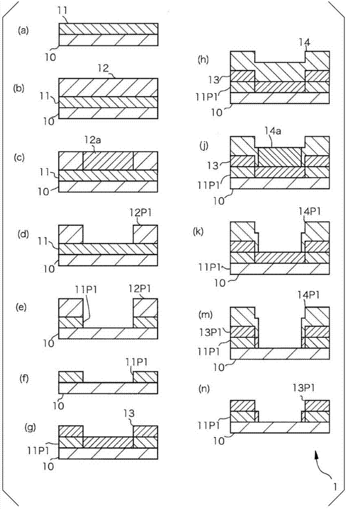
[0043] figure 1 It is a process drawing which schematically shows the manufacturing method of the phase shift mask which concerns on this embodiment.
[0044] The phase shift mask of this embodiment is comprised as the mask for patterning with respect to the glass substrate for FPDs, for example. As will be described later, in the patterning of the glass substrate using this mask, the composite wavelength of i-line, h-line, and g-line is used for exposure light.
[0045] In the manufacturing method of the phase shift mask according to the present embodiment, first, as figure 1 As shown in (a), the light shielding layer 11 is formed on the transparent substrate 10 .
[0046] As the transparent substrate 10, a material excellent in transparency and optical isotropy, for example, a quartz glass substrate is used. The size of the ...
no. 2 approach
[0089] Figure 4 It is a process drawing explaining the manufacturing method of the phase shift mask which concerns on 2nd Embodiment of this invention. In addition, in Figure 4 in, for with figure 1 Corresponding parts are denoted by the same symbols, and detailed description thereof will be omitted.
[0090] The phase shift mask 2 of the present embodiment ( Figure 4 (J)) has an alignment mark for alignment in the peripheral part, and this alignment mark is formed by the light-shielding layer 11P2. Next, the manufacturing method of the phase shift mask 2 is demonstrated.
[0091] First, a light-shielding layer 11 is formed on a transparent substrate 10 ( Figure 4 (A)). Next, a photoresist layer 12 is formed on the light shielding layer 11 ( Figure 4 (B)). The photoresist layer 12 can be positive type or negative type. Next, by exposing and developing the photoresist layer 12, a resist pattern 12P2 is formed on the light shielding layer 11 ( Figure 4 (C)).
[...
PUM
| Property | Measurement | Unit |
|---|---|---|
| Thickness | aaaaa | aaaaa |
Abstract
Description
Claims
Application Information
 - R&D
- Intellectual Property
- Life Sciences
- Materials
- Tech Scout
- Unparalleled Data Quality
- Higher Quality Content
- 60% Fewer Hallucinations
Browse by: Latest US Patents, China's latest patents, Technical Efficacy Thesaurus, Application Domain, Technology Topic, Popular Technical Reports.
© 2025 PatSnap. All rights reserved.Legal|Privacy policy|Modern Slavery Act Transparency Statement|Sitemap|About US| Contact US: help@patsnap.com


