Thin film transistor manufacturing method

A technology of thin film transistors and manufacturing methods, which is applied in the field of Lig, can solve the problems of uniformity reduction, influence on TFT electrical properties, influence on gate oxide layer thickness and step coverage, etc., to improve uniformity, reduce bump height, and display effect better effect

Inactive Publication Date: 2015-07-01
KUNSHAN NEW FLAT PANEL DISPLAY TECH CENT +1
View PDF4 Cites 17 Cited by
  • Summary
  • Abstract
  • Description
  • Claims
  • Application Information

AI Technical Summary

Problems solved by technology

[0002] At present, the LTPS (Low Temperature Poly-silicon, low-temperature polysilicon) backplane preparation technology mainly adopts the mainstream crystallization technology of ELA (Excimer Laser Annealer, excimer laser annealing). Under the irradiation of high-energy laser, a-Si (amorphous Silicon) recrystallized to generate Poly (polysilicon), but this layer of Poly film has obvious protrusions at the grain boundary of polysilicon, which affects the thickness and step coverage of the subsequent gate oxide la

Method used


Image

  • Thin film transistor manufacturing method
  • Thin film transistor manufacturing method
  • Thin film transistor manufacturing method

Examples


Embodiment Construction

[0027] In order to facilitate a further understanding of the method and the achieved effects of the present invention, preferred embodiments are described in detail below in conjunction with the accompanying drawings.

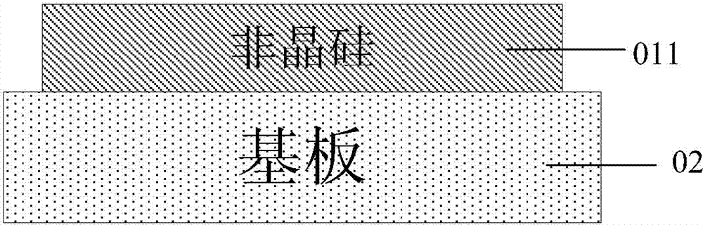
[0028] refer to Figure 8 The process flow chart of the present invention and other drawings of the present invention, first utilize CVD (Chemical Vapor Deposition, chemical vapor deposition) deposition method to deposit a layer of amorphous silicon 011 on the TFT substrate 02, such as figure 1 As shown in the schematic diagram of the deposition structure, the substrate 02 is a glass substrate, and the thickness of the amorphous silicon 011 film is 300-1000 Å.

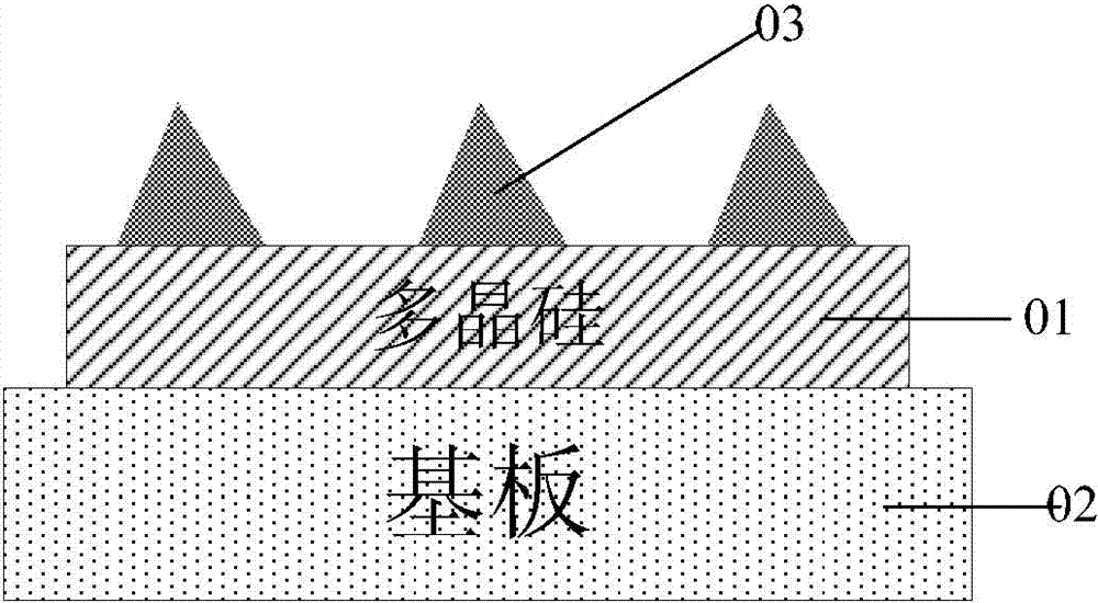
[0029] Use ELA (excimer laser annealing) technology to crystallize amorphous silicon 011 to become polysilicon 01. During the crystallization process, a large number of protrusions 03 are generated on the surface of polysilicon 01 due to ELA crystallization, such as figure 2 Shown is a schematic stru...


PUM


Abstract

The invention discloses a thin film transistor manufacturing method, which comprises the following steps: (1) a chemical vapor deposition method is firstly used for depositing a layer of amorphous silicon on the substrate of the thin film transistor; (2) excimer laser annealer (ELA) technology is used for crystallizing the amorphous silicon to form poly-silicon, and during the crystallizing process, a large number of ridges caused by laser annealing crystallizing are generated on the surface of the poly-silicon; (3) a coating mode is used for manufacturing a flattening layer on the poly-silicon with the ridges to enable the flattening layer to fully cover the ridges of the poly-silicon; and (4) etching is carried out on the flattening layer, when the ridges are etched, the flattening layer and the ridges are etched altogether, and a remaining flattening layer and a remaining small number of ridges are left on the poly-silicon. By adopting the thin film transistor manufacturing method of the invention, the ridge height of the poly-silicon after ELA crystallizing can be greatly reduced, uniformity of AMOLED (Active Matrix Organic Light Emitting Diode) backplane can be improved, and display effects are better.

Description

technical field [0001] The present invention relates to a method for manufacturing a thin film transistor (TFT, Thin Film Transistor) in an active matrix organic light emitting display (AMOLED, Active Matrix Organic Light Emitting Diode), in particular to a method that can effectively reduce excimer laser annealing polysilicon protrusions. A method of fabricating a highly advanced thin film transistor. Background technique [0002] At present, the LTPS (Low Temperature Poly-silicon, low-temperature polysilicon) backplane preparation technology mainly adopts the mainstream crystallization technology of ELA (Excimer Laser Annealer, excimer laser annealing). Under the irradiation of high-energy laser, a-Si (amorphous Silicon) is recrystallized to generate Poly (polysilicon), but this layer of Poly film has obvious protrusions at the grain boundaries of polysilicon, which affects the thickness and step coverage of the subsequent gate oxide layer, mainly affecting the electrical...

Claims


Application Information

Patent Timeline
IPC IPC(8): H01L21/336H01L29/786
CPCH01L27/1214H01L29/66772H01L29/786H10K59/12
Inventor 赵景训
Owner KUNSHAN NEW FLAT PANEL DISPLAY TECH CENT
Why Eureka
Try Eureka