A super-corrosion-resistant nickel-chrome plated part and its manufacturing method
A manufacturing method and nickel plating technology, applied in the direction of chemical instruments and methods, metal layered products, layered products, etc., can solve the problems of collinear production of hexavalent chromium and trivalent chromium, inapplicability of products, and improvement of corrosion resistance Limited and other issues
- Summary
- Abstract
- Description
- Claims
- Application Information
AI Technical Summary
Problems solved by technology
Method used
Image
Examples
Embodiment 1
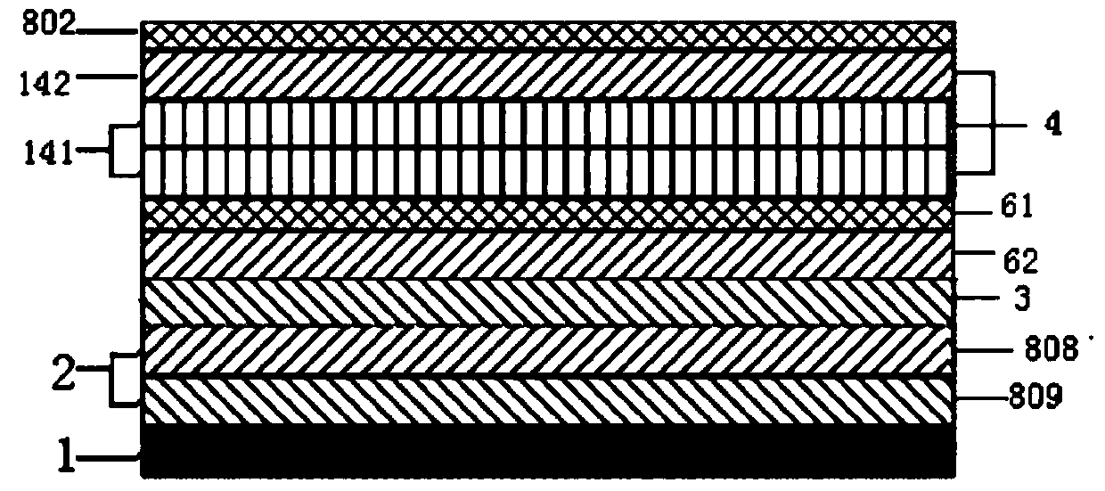
[0080] Substrate 1 (ABS material); Pretreatment coating 2 comprises chemical nickel layer 809, making a bottom nickel layer 808, and chemical nickel layer 809 is deposited on the whole substrate 1, and making bottom nickel layer 808 is deposited on the chemical nickel layer 809, in A copper-plated layer 3 is formed on the bottom nickel layer 808; a semi-gloss nickel layer 62, which is formed on the copper-plate layer 3; and a full-gloss nickel layer 61, which is formed on the semi-gloss nickel layer 62; and a functional layer 4, It is formed on the all-optical nickel layer 61, wherein the functional layer 4 includes a low-potential nickel layer 141 and a microporous nickel layer 142 formed on the low-potential nickel layer, wherein the low-potential nickel layer 141 is a high-sulfur nickel layer, which is formed on on the full-gloss nickel layer 61; and a decoration layer 802, which is formed on the microporous nickel layer 142, and the decoration layer 802 is a trivalent white...
Embodiment 2
[0082] Substrate 1 (ABS material); Pretreatment coating 2 comprises chemical nickel layer 809, making a bottom nickel layer 808, and chemical nickel layer 809 is deposited on the whole substrate 1, and making bottom nickel layer 808 is deposited on the chemical nickel layer 809, in A copper-plated layer 3 is formed on the bottom nickel layer 808; a semi-gloss nickel layer 62, which is formed on the copper-plate layer 3; and a full-gloss nickel layer 61, which is formed on the semi-gloss nickel layer 62; and a functional layer 4, It is formed on the all-optical nickel layer 61, wherein the functional layer 4 includes a low-potential nickel layer 141 and a microporous nickel layer 142 formed on the low-potential nickel layer, wherein the low-potential nickel layer 141 is a micro-crack nickel layer, which is formed on on the full-gloss nickel layer 61; and a decoration layer 802, which is formed on the microporous nickel layer 142, and the decoration layer 802 is a trivalent black...
Embodiment 3
[0084] Substrate 1 (ABS material); Pretreatment coating 2 comprises chemical nickel layer 809, making a bottom nickel layer 808, and chemical nickel layer 809 is deposited on the whole substrate 1, and making bottom nickel layer 808 is deposited on the chemical nickel layer 809, in A copper-plated layer 3 is formed on the bottom nickel layer 808; a semi-gloss nickel layer 62, which is formed on the copper-plate layer 3; and a full-gloss nickel layer 61, which is formed on the semi-gloss nickel layer 62; and a functional layer 4, It is formed on the all-optical nickel layer 61, wherein the functional layer 4 includes a low-potential nickel layer 141 and a microporous nickel layer 142 formed on the low-potential nickel layer, wherein the low-potential nickel layer 141 is a micro-crack nickel layer, which is formed on All-light nickel layer 61 is a high-sulfur nickel layer and microcrack nickel layer (can be that high-sulfur nickel layer is formed on all-light nickel layer or sati...
PUM
| Property | Measurement | Unit |
|---|---|---|
| thickness | aaaaa | aaaaa |
| thickness | aaaaa | aaaaa |
| thickness | aaaaa | aaaaa |
Abstract
Description
Claims
Application Information


