Polyresistor manufacturing method and polyresistor

A technology of polycrystalline resistors and manufacturing methods, applied in semiconductor/solid-state device manufacturing, circuits, electrical components, etc., can solve problems such as increased process complexity, polycrystalline poly damage, unfavorable resistance stability, etc., so as to save etching and cleaning process, the effect of saving production costs

Active Publication Date: 2015-07-22
FOUNDER MICROELECTRONICS INT
View PDF5 Cites 1 Cited by
  • Summary
  • Abstract
  • Description
  • Claims
  • Application Information

AI Technical Summary

Problems solved by technology

[0004] However, since the two layers of silicon nitride are etched separately, the complexity of the process is increased
In addition, since the contact hole window of the polycrystalline poly resistance is also etched during the process of etching the top layer of silicon nitride, the polycrystalline poly will be damaged during the process of etching the contact hole, which is not conducive to the stability of the resistance.

Method used


Image

  • Polyresistor manufacturing method and polyresistor
  • Polyresistor manufacturing method and polyresistor
  • Polyresistor manufacturing method and polyresistor

Examples


Embodiment Construction

[0018] In order to be able to understand the above objectives, features and advantages of the present invention more clearly, the present invention will be further described in detail below in conjunction with the accompanying drawings and specific embodiments. It should be noted that the embodiments of the application and the features in the embodiments can be combined with each other if there is no conflict.

[0019] In the following description, many specific details are set forth in order to fully understand the present invention. However, the present invention can also be implemented in other ways different from those described here. Therefore, the protection scope of the present invention is not limited to the specific details disclosed below. Limitations of the embodiment.

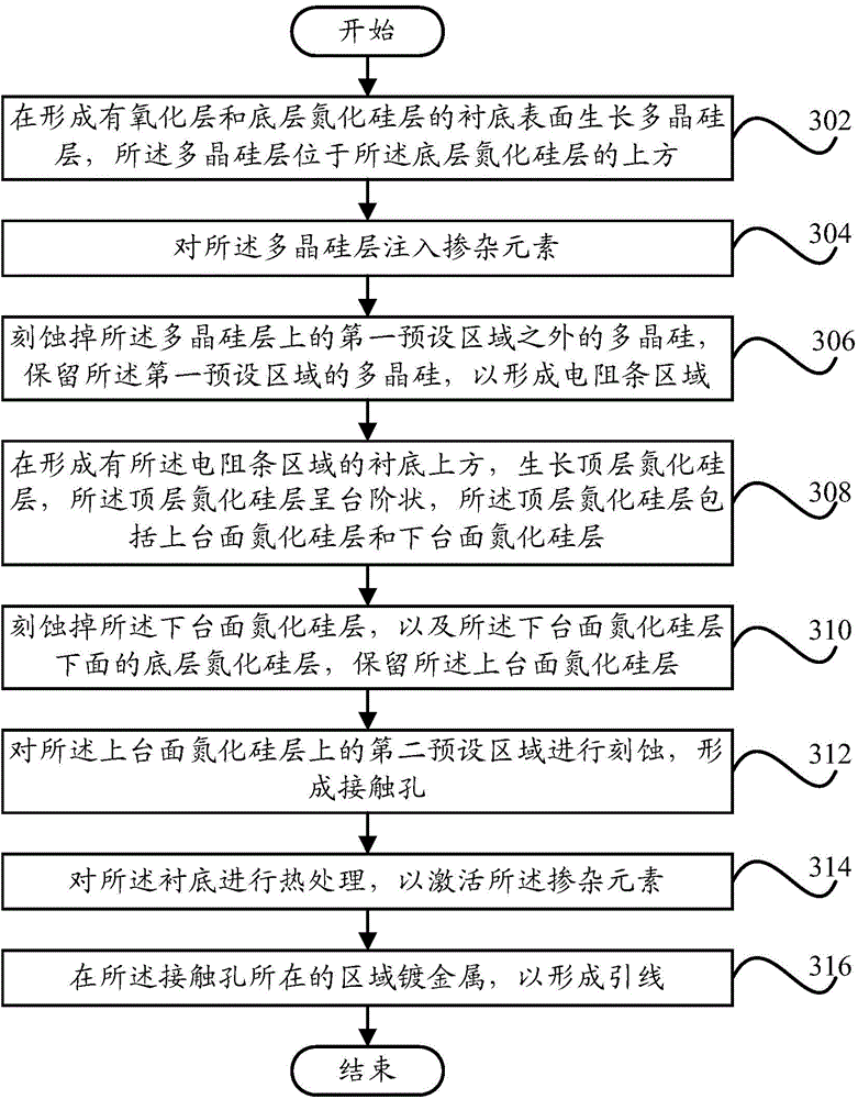
[0020] image 3 A schematic flowchart of a method for manufacturing a polycrystalline resistor according to an embodiment of the present invention is shown.

[0021] Such as image 3 As shown, the method ...


PUM

PropertyMeasurementUnit
thicknessaaaaaaaaaa
electrical resistivityaaaaaaaaaa
thicknessaaaaaaaaaa

Abstract

The invention provides a polyresistor manufacturing method and a polyresistor. The polyresistor manufacturing method comprises steps: a polycrystalline silicon layer grows on the surface of a substrate on which an oxide layer and a bottom silicon nitride layer are formed; doped elements are injected to the polycrystalline silicon layer; polycrystalline silicon on the polycrystalline silicon layer except a first preset region is etched, polycrystalline silicon on the first preset region is kept, and a resistance strip region is formed; a top silicon nitride layer grows above the substrate on which the resistance strip region is formed, wherein the top silicon nitride layer is step-shaped and comprises an upper table silicon nitride layer and a lower table silicon nitride layer; the lower table silicon nitride layer is etched and the bottom silicon nitride layer below the lower table silicon nitride layer is etched; a second preset region on the upper table silicon nitride layer is etched to form a contact hole; heat treatment is carried out on the substrate; and metal is plated on the region where the contact hole is to form a lead. Through the technical scheme of the invention, the production cost can be saved, and stability of the resistor is improved.

Description

Technical field [0001] The present invention relates to the field of semiconductor technology, in particular to a method for manufacturing a polycrystalline resistor and a polycrystalline resistor. Background technique [0002] Since the 1970s and early 1980s, Junction Field Effect Transistor (JFET) has been widely used. For example, it can be used as the input stage of an operational amplifier to obtain a few smaller than the best bipolar circuits. The magnitude of the input current can also be used as an analog switch and current source. [0003] In related technologies, the production process of a JFET that combines polysilicon (poly) high resistance and diode (Diode) mainly includes: growing a layer of polysilicon on the bottom silicon nitride, and the two share a layer of mask plate. After silicon lithography and etching, the top layer of silicon nitride is grown. Through the photomask of this layer, combined with the photolithography and etching process, the resistance struc...

Claims


Application Information

Patent Timeline
Patent Type & Authority Applications(China)
IPC IPC(8): H01L21/02H01L23/522
Inventor 由云鹏潘光燃石金成王焜文燕
Owner FOUNDER MICROELECTRONICS INT
Why Eureka
Try Eureka