Control circuit applied to SOI (silicon on insulator) CMOS (complementary metal oxide semiconductor) radiofrequency switches

A radio frequency switch and circuit technology, applied in the direction of electrical components, transmission systems, etc., can solve the problems of large steady-state current of the circuit and long time required to output negative voltage, and achieve small steady-state current, increased transient current, circuit design complex effects

Active Publication Date: 2015-07-22
广东拓思软件科学园有限公司
View PDF7 Cites 22 Cited by
  • Summary
  • Abstract
  • Description
  • Claims
  • Application Information

AI Technical Summary

Problems solved by technology

But the main disadvantage of this circuit is that it takes a long time to output a negative voltage, and the steady-state current in the circuit is relatively large during normal operation

Method used


Image

  • Control circuit applied to SOI (silicon on insulator) CMOS (complementary metal oxide semiconductor) radiofrequency switches
  • Control circuit applied to SOI (silicon on insulator) CMOS (complementary metal oxide semiconductor) radiofrequency switches
  • Control circuit applied to SOI (silicon on insulator) CMOS (complementary metal oxide semiconductor) radiofrequency switches

Examples


Embodiment 1

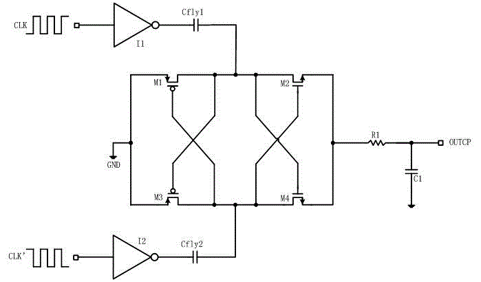
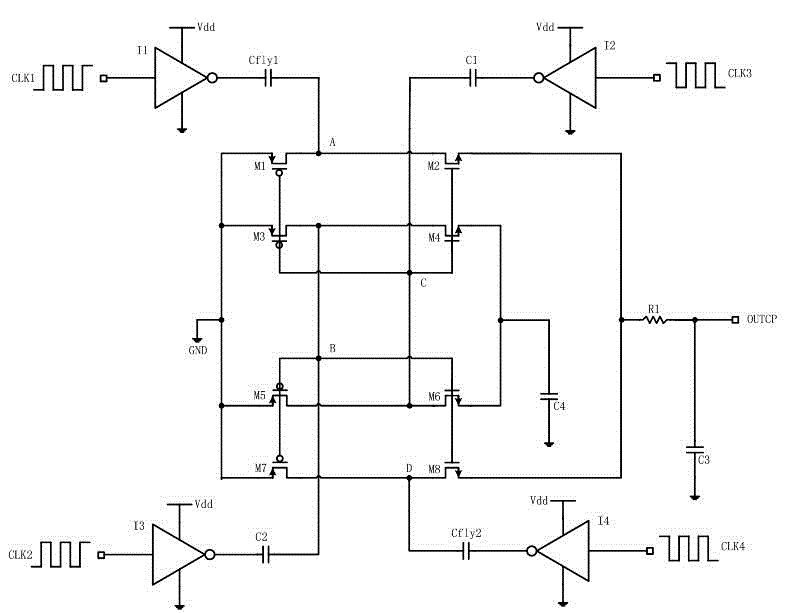
[0053] At the initial moment, that is, at the beginning of the first half period (0~T / 2) of the clock signal, the clock signal CLK1 and the clock signal CLK2 are at low level, then the output terminals of inverters I1 and I3 are at high level Vdd, that is, at the During the period of 0~T / 2, the power supply voltage charges the flying capacitor Cfly1 and capacitor C2 through the inverters I1 and I3 respectively. At this time, the voltage of the A node and the B node starts to rise from 0, and the clock signal CLK3 and the clock signal CLK4 are High level, low level at the output terminals of inverters I2 and I4, that is, within 0-T / 2 time, inverters I2 and I4 pull down the terminal voltage of capacitor C1 and flying capacitor Cfly2 to 0, this When the C node and D node voltages are both 0, within 0~T / 2 time, the first field effect transistor M1, the third field effect transistor M3, the fifth field effect transistor M5, the seventh field effect transistor M7, the second field ef...


PUM


Abstract

The invention discloses a control circuit applied to SOI (silicon on insulator) CMOS (complementary metal oxide semiconductor) radiofrequency switches. The control circuit comprises a band-gap reference circuit, a low-dropout linear voltage regulator, an annular oscillator, voltage inverters, a non-overlapping clock circuit, a charge pump and a level switching circuit. A core unit of the control circuit is a charge pump circuit capable of generating negative voltages. The band-gap reference circuit is connected with the low-dropout linear voltage regulator, an output end of the low-dropout linear voltage regulator is connected with the charge pump, an output end of the annular oscillator is connected with an input end of the inverter I2 by the inverter I1, an output end of the inverter I1 and an output end of the inverter I2 are connected with an input end of the non-overlapping clock generating circuit, four output ends of the non-overlapping clock generating circuit is connected with an input end of the charge pump, and the SOI CMOS radiofrequency switches can be controlled by an output end OUTPUT of the charge pump via the level switching circuit. The control circuit has the advantages that the charge pump capable of generating the negative voltages can be quickly started and has low steady-state currents, accordingly, radiofrequency switch tubes can be assuredly in excellent closed states under the conditions of high radiofrequency signals, and the linearity and the isolation of the radiofrequency switches can be improved.

Description

technical field [0001] The invention relates to the technical field of integrated circuits, in particular to a control circuit applied to SOI CMOS radio frequency switches. Background technique [0002] In a wireless communication transceiver, a high-performance switch is used for signal selection of the transmission path and the reception path, and its insertion loss, power capacity and other performances directly restrict the output power and noise figure performance of the entire system. In mobile terminal applications, the SOI CMOS process has performance comparable to that of the GaAs process, and because the SOI CMOS process can integrate circuits such as logic and controllers, and exhibit better ESD performance, it is widely used in high-performance RF switches Using SOI CMOS process. In the high-performance SOI CMOS RF switch control, negative voltage is often required to provide on-off control for the RF switch tube. How to generate a simple and reliable negative v...

Claims


Application Information

Patent Timeline
Patent Type & Authority Applications(China)
IPC IPC(8): H04B1/40
Inventor 刘斌陶亮章国豪
Owner 广东拓思软件科学园有限公司
Why Eureka
Try Eureka