Highly-efficient organic electroluminescent device based on fluorescence doped luminescent layer

A technology for electroluminescent devices and light-emitting layers, which can be used in electro-solid devices, electrical components, semiconductor devices, etc., and can solve problems such as low efficiency

Active Publication Date: 2015-08-12
JILIN YUANHE ELECTRONICS MATERIALS CO LTD
View PDF5 Cites 46 Cited by
  • Summary
  • Abstract
  • Description
  • Claims
  • Application Information

AI Technical Summary

Problems solved by technology

[0006] In order to solve the problem of low efficiency of traditional fluorescent dye devices, the purpose of the present invention is to use a thermally activated delayed fluorescent material with a singlet-triplet energy le

Method used


Image

  • Highly-efficient organic electroluminescent device based on fluorescence doped luminescent layer
  • Highly-efficient organic electroluminescent device based on fluorescence doped luminescent layer
  • Highly-efficient organic electroluminescent device based on fluorescence doped luminescent layer

Examples


Embodiment 1

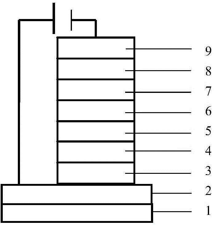
[0035] Example 1: Device [ITO / NPB / mCP / 4CzIPN:0.5%DFDB-QA / BCP / BePP 2 / LiF / Al]

[0036] The 15mm×15mm×1mm thick ITO conductive glass substrate was ultrasonically cleaned with ITO cleaning solution for 5 minutes, deionized water for 5 minutes, acetone for 20 minutes, and isopropanol for 20 minutes. After drying, plasma (plasma) treatment for 5 minutes. In high vacuum 5 x 10 -5 The hole transport layer NPB was sequentially deposited under Pa with a thickness of 35nm; the first exciton blocking layer mCP was deposited with a thickness of 5nm; the light emitting layer was deposited by dual-source co-evaporation, in which the host material was 4CzIPN and the guest doping material was DFDB-QA , the doping concentration is 0.5% (weight percentage), the thickness is 30nm; the second exciton blocking layer BCP, the thickness is 5nm; the electron transport layer BePP 2 , with a thickness of 40nm. Then deposit the electron injection layer LiF with a thickness of 1 nm; the metal cathode...

Embodiment 2

[0038] Example 2: Device [ITO / NPB / mCP / 4CzIPN:0.5%TCF 3 DB-QA / BCP / BePP 2 / LiF / Al]

[0039] The 15mm×15mm×1mm thick ITO conductive glass substrate was ultrasonically cleaned with ITO cleaning solution for 5 minutes, deionized water for 5 minutes, acetone for 20 minutes, and isopropanol for 20 minutes. After drying, plasma treatment for 5 minutes. In high vacuum 5 x 10 -5 The hole transport layer NPB was sequentially deposited under Pa with a thickness of 35nm; the first exciton blocking layer mCP was deposited with a thickness of 5nm; the light-emitting layer was deposited by double-source co-evaporation, in which the host material was 4CzIPN and the guest dopant material was TCF 3 DB-QA, the doping concentration is 0.5% (weight percentage), the thickness is 30nm; the second exciton blocking layer BCP, the thickness is 5nm; the electron transport layer BePP 2 , with a thickness of 40nm. Then deposit the electron injection layer LiF with a thickness of 1 nm and the metal cat...

Embodiment 3

[0041] Embodiment 3: Device [ITO / NPB / mCP / 4CzIPN:0.5%DCF 3 DB-QA / BCP / BePP 2 / LiF / Al]

[0042] The 15mm×15mm×1mm thick ITO conductive glass substrate was ultrasonically cleaned with ITO cleaning solution for 5 minutes, deionized water for 5 minutes, acetone for 20 minutes, and isopropanol for 20 minutes. After drying, plasma treatment for 5 minutes. In high vacuum 5 x 10 -5 The hole transport layer NPB was sequentially deposited under Pa with a thickness of 35nm; the first exciton blocking layer mCP was deposited with a thickness of 5nm; the light-emitting layer was deposited by double-source co-evaporation, in which the host material was 4CzIPN and the guest doping material was DCF 3 DB-QA, the doping concentration is 0.5% (weight percentage), the thickness is 30nm; the second exciton blocking layer BCP, the thickness is 5nm; the electron transport layer BePP 2 , with a thickness of 40nm. Then deposit the electron injection layer LiF with a thickness of 1 nm and the metal ...


PUM

PropertyMeasurementUnit
Band gap widthaaaaaaaaaa
Thicknessaaaaaaaaaa
Thicknessaaaaaaaaaa

Abstract

The invention relates to a device structure of an organic light-emitting diode (OLED), and especially relates to a highly-efficient organic electroluminescent device based on a fluorescence doped luminescent layer. The organic electroluminescent device comprises a transparent substrate, a transparent anode, a cavity transmission layer, a first exciton barrier layer, a luminescent layer, a second exciton barrier layer, an electronic transmission layer, an electronic injecting layer and a metal cathode. The luminescent layer is formed by mixing a main body and a guest body. The main body material is organic small molecules whose energy difference between a first kind single heavy excitation state and a triplet excitation state is quite small. The guest body material is dye molecules with high fluorescence efficiency, like quinacridone derivatives. The highly-efficient organic electroluminescent device based on a fluorescence doped luminescent layer is advantageous in that the external quantum efficiency exceeds 5% of theoretic limit efficiency of a conventional fluorescence device, and the luminescence efficiency of a fluorescent OLED device can be effectively improved; the luminescent device of the invention is high in brightness, low in starting voltage, high in efficiency, and low in efficiency roll-off.

Description

technical field [0001] The invention belongs to the technical field of organic electroluminescent devices, and in particular relates to an organic electroluminescent device (OLED). The organic electroluminescent device uses an organic material having thermally activated delayed fluorescence (TADF, Thermally Activated Delayed Fluorescence) characteristics as an organic material. The host material is doped with the quinacridone fluorescent material to prepare the light-emitting layer of the organic electroluminescent device, and the device has very high efficiency. Background technique [0002] Organic electroluminescent devices (OLEDs, Organic Light Emitting Diods) use the excitons generated by the recombination of electrons and holes to emit light. According to the statistical law of electron spin, it is speculated that the ratio of singlet excitons to triplet excitons produced by it is 1:3. Generally speaking, when using small molecule fluorescent light-emitting materials, ...

Claims


Application Information

Patent Timeline
IPC IPC(8): H01L51/50H01L51/54
CPCH10K85/60H10K85/6572H10K50/121H10K2101/20
Inventor 王悦
Owner JILIN YUANHE ELECTRONICS MATERIALS CO LTD
Why Eureka
Try Eureka