Method for forming varied doping region and device thereof

A technology of variable doping and edge, applied in the direction of electrical components, semiconductor/solid-state device manufacturing, circuits, etc., can solve the problems of high cost, complex formation process of variable doping regions, etc., and achieve reduced chip manufacturing costs and fewer photolithography times , the effect of simple process

Inactive Publication Date: 2015-08-19
PEKING UNIV FOUNDER GRP CO LTD +1
View PDF5 Cites 4 Cited by
  • Summary
  • Abstract
  • Description
  • Claims
  • Application Information

AI Technical Summary

Problems solved by technology

[0005] The present invention provides a method and device for forming a variable doping region to solve the technical problems of complex formation process and high cost of the variable doping region in the prior art

Method used


Image

  • Method for forming varied doping region and device thereof
  • Method for forming varied doping region and device thereof
  • Method for forming varied doping region and device thereof

Examples


Embodiment 1

[0063] The following takes the use of silicon nitride / silicon oxide / silicon nitride sandwich structure multi-layer composite film layer to form a variable doping region as an example to describe the specific implementation process of an embodiment of the present invention in detail, see Figure 8 .

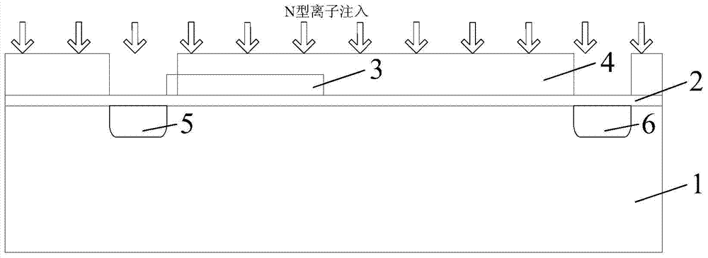
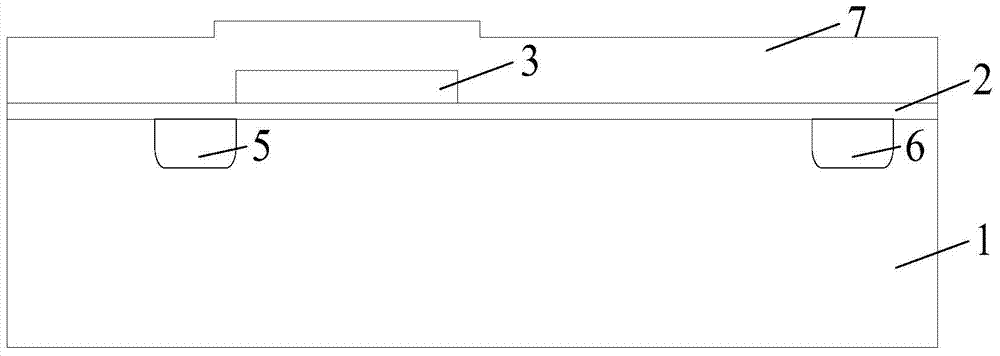
[0064] Step 801: Fabricate gate oxide layer 2 and polysilicon 3 gate on P-type substrate 1, form N+ source and drain regions, and grow a sandwich structure of silicon nitride / silicon oxide / silicon nitride multilayer on the gate oxide layer and polysilicon surface Composite film layer.

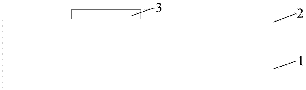
[0065] The schematic diagram of making gate oxide layer 2 and polysilicon 3 is shown in figure 1 , the growth temperature of the gate oxide layer 2 is about 900-1100° C., and the thickness is about 0.05-0.20 μm; the growth temperature of the polysilicon 3 is about 500-700° C., and the thickness is about 0.3-0.8 μm.

[0066] see figure 2 Phosphorus or arsenic ions are implanted after photolithog...


PUM

PropertyMeasurementUnit
thicknessaaaaaaaaaa
temperatureaaaaaaaaaa
thicknessaaaaaaaaaa

Abstract

The invention provides a method for forming a varied doping region and a device thereof. The method comprises the steps of growing a multilayer composite film on the surfaces of a gate and a gate oxide layer, wherein the multilayer composite film comprises at least two dielectric layers which are made of different materials, namely a first dielectric layer and a second dielectric layer, furthermore a corresponding step is formed by the dielectric layers because of existence of the gate; performing photolithography for exposing the surface of the first dielectric layer in an area which corresponds with the area from the gate edge to the drain edge, performing primary ion implantation in an area from the step edge to the drain edge on the first dielectric layer, thereby forming a first varied doping region; etching the surface of the second dielectric layer in an area which corresponds with the area from the gate edge to the drain edge, performing secondary ion implantation in an area from the step edge to the drain edge on the second dielectric layer, thereby forming a second varied doping region; and etching the surface of the gate oxide layer in an area which corresponds with the area from the gate edge to the drain edge, and performing third ion implantation in an area from the gate edge to the drain edge, thereby forming a third varied doping region. Compared with the prior art, the method of the invention is advantageous in that the cost is reduced.

Description

technical field [0001] The invention relates to the technical field of semiconductor chip manufacturing technology, in particular to a method and device for forming a variable doping region. Background technique [0002] In the formation process of the variable doping region, the prior art generally adopts multiple photolithography etching methods to produce multi-level steps, and then utilizes the different step heights to have different shielding capabilities for ion implantation to form variable doping regions. region, the specific method is: making gate oxide layer 2 and polysilicon 3 on P-type substrate 1, see figure 1 ; Perform photolithography and N-type ion implantation on the gate oxide layer 2 and polysilicon 3 to form N+ source region 5 and N+ drain region 6, such as figure 2 As shown, 4 is a photoresist; a dielectric layer 7 is grown on the gate oxide layer 2 and polysilicon 3, see image 3 ; The dielectric layer 7 is etched multiple times to form multi-level ...

Claims


Application Information

Patent Timeline
Patent Type & Authority Applications(China)
IPC IPC(8): H01L21/336
CPCH01L21/265H01L29/06H01L29/66477
Inventor 马万里
Owner PEKING UNIV FOUNDER GRP CO LTD
Why Eureka
Try Eureka