A kind of vertical structure LED chip preparation method

A LED chip and vertical structure technology, applied in the direction of electrical components, circuits, semiconductor devices, etc., can solve the problems of uneven energy, large leakage of processed chips, and high voltage of vertical structure chips, so as to reduce the damage of internal stress and solve the problem of etching The effect of uneven depth, avoiding high voltage and leakage

Inactive Publication Date: 2017-06-09
西安利科光电科技有限公司
View PDF5 Cites 0 Cited by
  • Summary
  • Abstract
  • Description
  • Claims
  • Application Information

AI Technical Summary

Problems solved by technology

One of the biggest problems encountered at present is that more defects and stress are generated during the growth process of GaN-based epitaxial wafers. During the wafer bonding process, the temperature needs to be raised. When the temperature is lowered, the number of defects in GaN will further increase and the number of internal defects will increase. The stress is further increased, so the wafer bonding process will damage the GaN epitaxial layer, resulting in large chip leakage; the second is to use the laser lift-off technology to scan the wafer through the focused laser spot, and the distance between the spot and the spot during scanning is The overlapping will lead to energy unevenness, and the uniformity of the process is poor, resulting in uneven peeling of the GaN / sapphire interface, which leads to low laser peeling yield and large leakage of processed chips; the third is the process of manufacturing N electrodes after laser peeling In the process, the N-type GaN layer needs to be etched by ICP. Since the N-type GaN surface is rough and uneven after laser lift-off, it is difficult to control the etching depth during the ICP etching process, which will cause high voltage and leakage of the vertical structure chip. bigger

Method used


Image

  • A kind of vertical structure LED chip preparation method
  • A kind of vertical structure LED chip preparation method

Examples


preparation example Construction

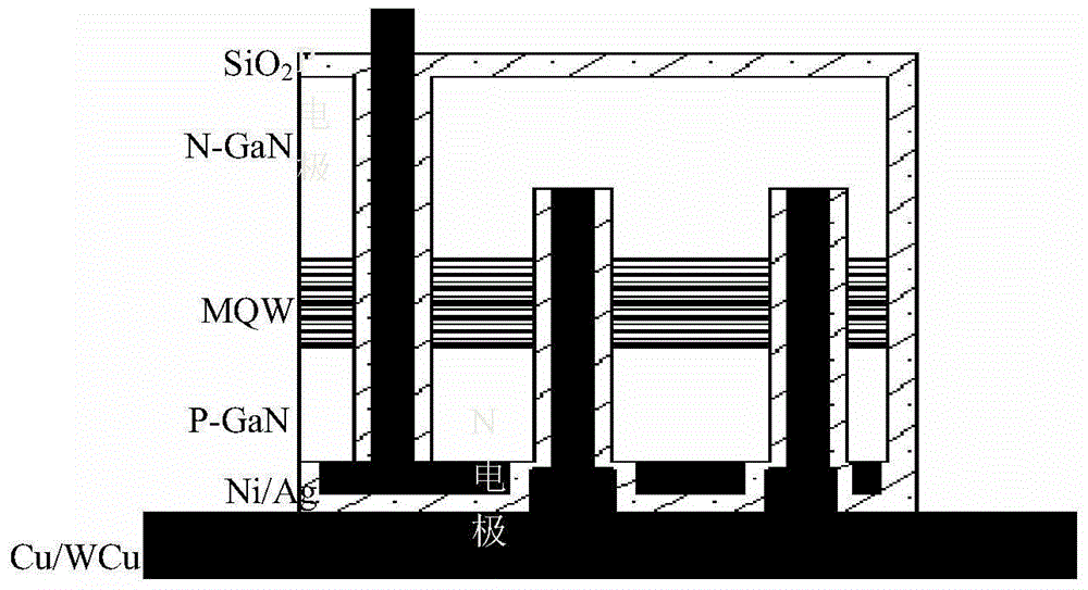
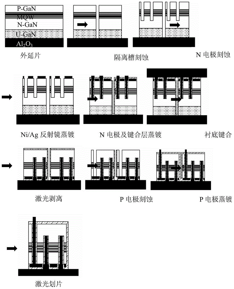
[0040] The method for preparing a vertical structure LED chip of the present invention mainly includes the following steps:

[0041] (1) Isolation groove etching: put the epitaxial wafer into the ICP etching equipment for isolation groove etching. The epitaxial wafer can be flat epitaxial wafer, PSS epitaxial wafer, secondary corroded epitaxial wafer or epitaxial wafer prepared by other methods. The etching depth is from the epitaxial wafer surface to the sapphire substrate Al 2 o 3 On the surface, silicon oxide and photoresist are used to mask the area outside the isolation groove during etching, and hot acid H is used after etching 2 SO 4 :H 3 PO 4 = Soak the 3:1 solution at 200-250°C for 3-5 minutes to form a chip isolation groove.

[0042] (2) N electrode etching and mirror evaporation: use ICP etching technology for traditional N electrode etching; use electron beam evaporation machine for mirror evaporation (Ni / Ag or Ni / Al), evaporation The edge of the covered area...


PUM


Abstract

In order to raise the processing yield of vertical-structure LED chips, the present invention provides a novel method for manufacturing the-vertical structure LED chips, which can notably reduce electric leakage of the chips and raise the chip production yield. A P electrode of the chip is formed on the surface of the chip, an N electrode of the chip is bonded with a silicon / copper / tungsten copper alloy substrate, and the P electrode is welded with a support during packaging of the chip. Combination of the ICP etching technique and the hot acid corrosion technology is adopted to form chip isolation channels. A laser spot is adjusted during laser stripping so as to be matched in size with the chip after the isolating channels are formed. An epitaxial wafer is bonded on the silicon / copper / tungsten copper alloy substrate through a high-temperature bonding technique, the ultrasonic technology is then used, and by using internal stress produced in the bonding process and the ultrasonic vibration technology, separation of gallium nitride and the substrate is further raised.

Description

[0001] Technical field: [0002] The invention relates to a method for preparing a vertical structure LED chip, belonging to the field of LED chip preparation. [0003] Background technique: [0004] LED has become the third-generation lighting source after incandescent lamps and fluorescent lamps. Compared with traditional lighting sources, LED semiconductor lighting sources have the following advantages: high luminous efficiency, small size, long life, energy saving, and environmental protection. At present, one of the main reasons why LEDs have not entered general lighting on a large scale is that LED luminous efficiency and heat dissipation conditions need to be further improved, and the second is to reduce the production cost of LEDs. Since the vertical structure LED satisfies good heat dissipation conditions, it can be driven with a larger current, thereby improving the LED luminous efficiency. Therefore, the vertical structure LED will accelerate the process of LED app...

Claims


Application Information

Patent Timeline
Patent Type & Authority Patents(China)
IPC IPC(8): H01L33/00
CPCH01L33/005H01L33/36
Inventor 宁磊
Owner 西安利科光电科技有限公司
Why Eureka
Try Eureka