Flip LED chip and manufacturing method thereof

A technology of LED chips and manufacturing methods, applied in electrical components, circuits, semiconductor devices, etc., can solve problems such as large difficulty coefficients, and achieve the effects of low preparation cost, low process complexity, and large-scale mass production.

Inactive Publication Date: 2015-08-26
ENRAYTEK OPTOELECTRONICS
View PDF3 Cites 7 Cited by
  • Summary
  • Abstract
  • Description
  • Claims
  • Application Information

AI Technical Summary

Problems solved by technology

Difficulties mainly include the need to protect the front structure of the chip, the need to prepare additional masks, and strict control of process conditions. Therefore, the degree of difficulty is relatively high
In addition, the flip-chip LED chip prepared by thinning the sapphire substrate does not roughen the light-emitting surface.

Method used


Image

  • Flip LED chip and manufacturing method thereof
  • Flip LED chip and manufacturing method thereof
  • Flip LED chip and manufacturing method thereof

Examples


Embodiment Construction

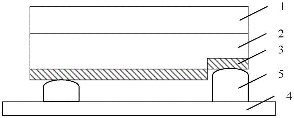
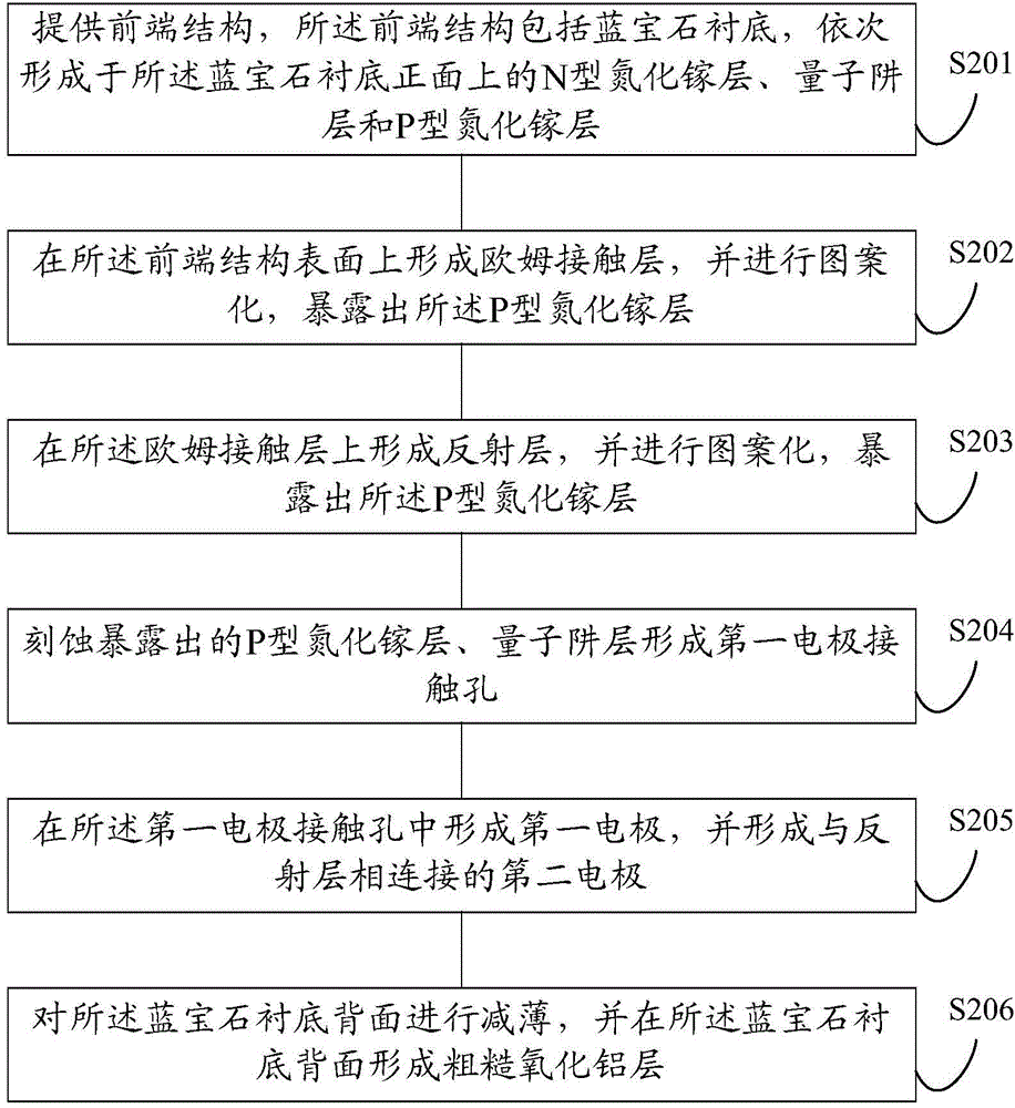
[0030] The flip-chip LED chip of the present invention and its manufacturing method will be described in more detail below in conjunction with schematic diagrams, wherein a preferred embodiment of the present invention is shown, and it should be understood that those skilled in the art can modify the present invention described here and still implement the present invention. Beneficial effects of the invention. Therefore, the following description should be understood as the broad knowledge of those skilled in the art, but not as a limitation of the present invention.

[0031] In the interest of clarity, not all features of an actual implementation are described. In the following description, well-known functions and constructions are not described in detail since they would obscure the invention with unnecessary detail. It should be appreciated that in the development of any actual embodiment, numerous implementation details must be worked out to achieve the developer's spec...


PUM


Abstract

The invention discloses a flip LED chip and a manufacturing method thereof. A front-end structure containing a sapphire substrate, an N type gallium nitride layer, a quantum well layer, and a P type gallium nitride layer is provided, wherein the N type gallium nitride layer, the quantum well layer, and the P type gallium nitride layer are formed on the front side of the sapphire substrate; an ohmic contact layer and a reflecting layer are formed on the front-end structure; a first electrode connecting the N type gallium nitride layer and a second electrode connecting the reflecting layer are formed; and reduction processing is carried out on the back side of the sapphire substrate and a rough aluminium oxide layer is formed. Compared with the prior art, because of the aluminium oxide layer with the rough surface and the material consistent with the substrate material, an effect of improvement of the luminous efficiency based on surface roughening is realized; and defects of great influence on the front side and high cost in the prior art can be overcome. Therefore, the preparation cost is low; the process complexity is low; and the large-scale mass production can be realized easily.

Description

technical field [0001] The invention relates to the technical field of semiconductors, in particular to a flip-chip LED chip and a manufacturing method thereof. Background technique [0002] For traditional front-mounted LED chips, P-type GaN is difficult to dope, resulting in low hole carrier concentration and difficulty in growing thick, resulting in difficult diffusion of current. At present, the method of preparing ultra-thin metal film or ITO film on the surface of P-type GaN is generally used to achieve The current has to spread evenly. However, the metal thin film electrode layer has to absorb part of the light to reduce the light extraction efficiency, and if the thickness is reduced, it will in turn limit the current diffusion layer to achieve uniform and reliable current diffusion on the surface of the P-type GaN layer. Although the light transmittance of ITO is as high as 90%, the electrical conductivity is not as good as that of metal, and the diffusion effect o...

Claims


Application Information

Patent Timeline
IPC IPC(8): H01L33/00H01L33/44
CPCH01L33/007H01L33/44
Inventor 李智勇徐慧文李起鸣张宇
Owner ENRAYTEK OPTOELECTRONICS
Why Eureka
Try Eureka