
Gold nanoparticle surface plasmon polariton-based crystalline silicon heterojunction with intrinsic thin-layer (HIT) solar cell

A solar cell, gold nanoparticle technology, applied in circuits, photovoltaic power generation, electrical components, etc., to achieve high short-circuit current, promote scattering and absorption, and improve photoelectric conversion efficiency.

Inactive Publication Date: 2015-09-09
JIANGNAN UNIV
View PDF5 Cites 6 Cited by
  • Summary
  • Abstract
  • Description
  • Claims
  • Application Information

AI Technical Summary

Problems solved by technology

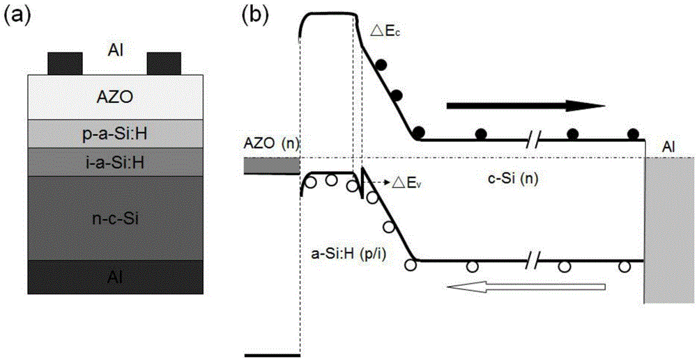
But usually the work function of the transparent conductive layer indium tin oxide (Indium Tin Oxide: ITO) is in the range of 4.4-4.9eV, while that of AZO is lower

Method used


Image

  • Gold nanoparticle surface plasmon polariton-based crystalline silicon heterojunction with intrinsic thin-layer (HIT) solar cell
  • Gold nanoparticle surface plasmon polariton-based crystalline silicon heterojunction with intrinsic thin-layer (HIT) solar cell

Examples


Embodiment Construction

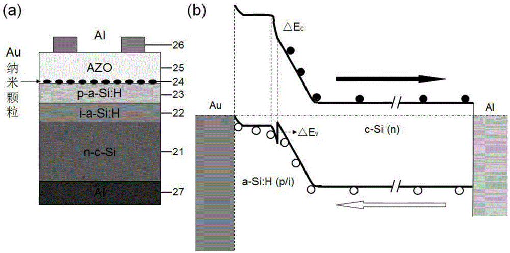
[0020] The present invention adopts plasma enhanced chemical vapor deposition method (including capacitive coupling and inductively coupled plasma) to prepare intrinsic and p-type a-Si:H. Generally, intrinsic amorphous silicon and p-type amorphous silicon are grown in two vacuum chambers; intrinsic amorphous silicon uses SiH 4 +H 2 As the reactive gas, while the p-type emitter junction uses SiH 4 +H 2 +B 2 H 6 as a reactive gas. After preparing the emitter junction p-a-Si:H, the sample is sent to the magnetron sputtering chamber through a vacuum transfer system, and a discontinuous ultra-thin gold film (5-10) is deposited on the surface of the emitter junction by controlling the magnetron sputtering process. Nanometer), and then directly perform the subsequent annealing process in the vacuum chamber to make the gold film curl into nanoparticles, and obtain the uniform distribution of Au-NPs on the p-a-Si:H layer film. Then, the transparent conductive film and the front a...


PUM

PropertyMeasurementUnit
electron work functionaaaaaaaaaa
thicknessaaaaaaaaaa
thicknessaaaaaaaaaa

Abstract

The invention relates to an optimization method of an n type crystalline silicon heterojunction with intrinsic thin-layer (HIT) solar cell structure. According to the optimization method, gold nanoparticles (Au-NPs) are inlaid between a p type emission layer (p-a-Si:H) and a transparent electric conduction film (n-AZO), so that the interface electrical transmission characteristics of the p type emission layer and the transparent electric conduction film can be improved, and the efficiency of the HIT cell can be improved; a high-work function considering optical and electrical properties both is adopted, and therefore, the solving of the problem of blocking of carrier transport by a schottky barrier which is caused by mismatch of work functions of the p type emission layer and the n type AZO can be facilitated, and surface plasmon polaritons can be formed, and the scattering and absorption of light in cell can be enhanced through the resonance effect of the surface plasmon polaritons, and thus, the photoelectric conversion efficiency of the HIT cell can be further improved. The optimization method of the invention can be applied to efficient single-junction and double-junction crystalline silicon HIT solar cells and interdigitated back contact type (IBC) heterojunction solar cells.

Description

technical field [0001] The invention provides an n-type crystalline silicon HIT solar cell structure based on surface plasmon of gold nanoparticles (Au-NPs), belonging to the technical field of solar cells and photovoltaics, and can be applied to various high-efficiency crystalline silicon heterojunction solar cells Cells include single- and double-junction HIT solar cells, interleaved back-contact (IBC) heterojunction solar cells. Background technique [0002] With the shortage of energy and people's requirements for a friendly environment, more and more countries are turning their attention to clean and renewable energy, especially photovoltaic solar energy. Silicon-based heterojunction solar cells combine the high conversion efficiency and high stability of conventional crystalline silicon cells with the characteristics of low-temperature growth process of thin-film cells, and are a hot spot in the field of high-efficiency cell research today. The HIT crystalline silicon...

Claims


Application Information

Patent Timeline
Patent Type & Authority Applications(China)
IPC IPC(8): H01L31/0352H01L31/068
CPCH01L31/0352H01L31/0682Y02E10/547
Inventor 肖少庆姚尧顾晓峰张秀梅丁荣
Owner JIANGNAN UNIV
Learn More