Radio frequency and band-shaped wire interface assembly method

An assembly method and stripline technology, applied in electrical components, circuits, waveguide-type devices, etc., can solve problems such as the inability to know the theoretical and physical design methods, the design of high-speed signal interfaces, and the lack of complete design methods. , to achieve the effect of reducing space volume and design difficulty, fast signal transmission, and reducing the space required for wiring and bending

Inactive Publication Date: 2015-09-16
10TH RES INST OF CETC
View PDF2 Cites 4 Cited by
  • Summary
  • Abstract
  • Description
  • Claims
  • Application Information

AI Technical Summary

Problems solved by technology

The shortcomings of this document are that it is limited to theoretical analysis, it is impossible to know the design method of theory and objects, and it does not have the realizability of a complete function.
This paper introduces the basic characteristics of high-frequency substrate materials and three kinds of high-frequency substrate physical properties, analyzes the way to avoid the transmission effect of high-speed circuits, summarizes the key points of wiring design of high-speed printed circuit boards, and puts forward wiring improvement actions and preventive measures. The insufficiency of the literature is that it only summarizes from the perspective of production, does not combine design with production, and does not design high-speed signal interface design, which has no reference value for interface design
Introduced the basic theory of signal integrity and the signal integrity simulation process based on the simulation software Hyperlynx, focused on how to use the high-speed PCB design method

Method used


Image

  • Radio frequency and band-shaped wire interface assembly method
  • Radio frequency and band-shaped wire interface assembly method
  • Radio frequency and band-shaped wire interface assembly method

Examples


Embodiment Construction

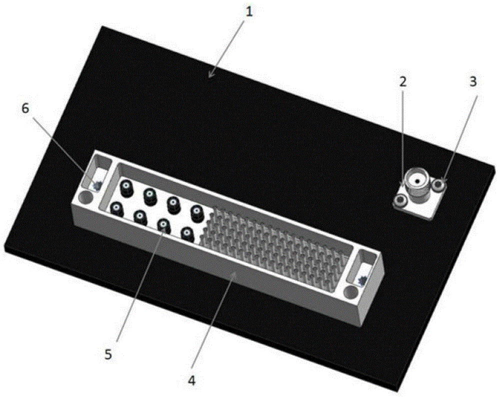
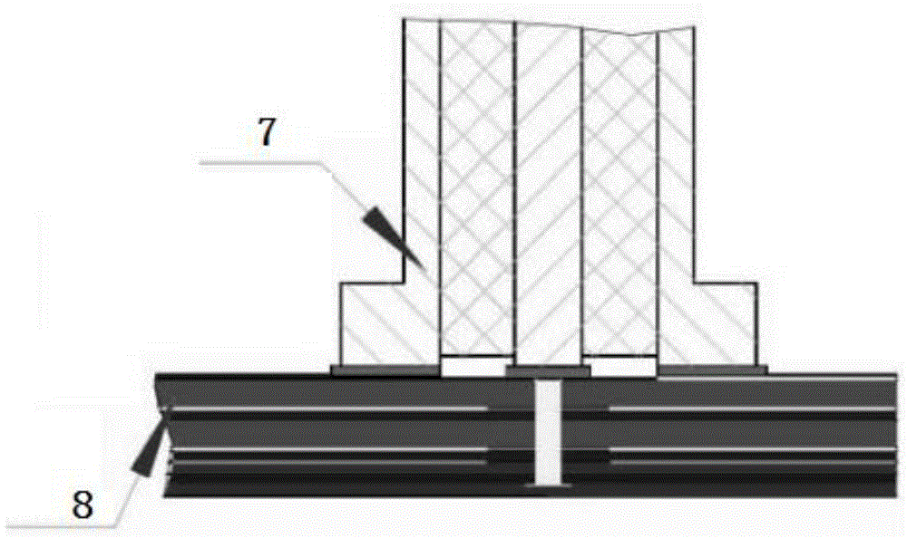
[0024] refer to Figure 1-Figure 3 . In a best implementation case described below, the broadband microwave backplane operating in the 6GHz frequency range, the assembly structure of the RF connector on the broadband microwave backplane mainly includes the broadband microwave backplane, connected through strip lines and metalized holes Arrayed high-frequency connectors 5, independent high-frequency connectors 2 and low-frequency connectors 4 together. The broadband microwave backplane serving as the high-frequency connector bearing layer and high-frequency interconnection is provided with soldering pads for connector welding. Large-area metal ground and metal transmission lines are all copper layers. The weldable areas on the upper and lower surfaces of the broadband microwave backplane are interconnected with the internal striplines of the broadband microwave backplane through metallized holes. Solder paste is used to realize the brazing assembly of the high-frequency sock...


PUM


Abstract

The invention discloses a radio frequency and band-shaped wire interface assembly method, which is high in transmission efficiency, small in loss, reliable in performance and high in integration interconnection density. The radio frequency and band shape wire interface assembly method can be realized through steps of integrating a high frequency signal member and a low frequency member through a broadband microwave backboard to form a motherboard, and placing a high frequency connector and an LAM connector on a same plane of a same plane layer, expanding into a stack of layers of a three-dimensional circuit toward a z direction through interlayer vertical interconnection by the planar circuit printed with the circuit graphs, in a radio frequency portion, adopting signals between Rogers RO6002 core board layers and performing radio frequency connection through metalized hole interconnection structure between the stack layers of the core plates, realizing signal transmission between the radio frequency layers through the layer pressure, realizing electric communication by a high frequency connector 2 and a high frequency connector 5 through a surface welding disc of a broadband microwave backboard 1 and manufacturing a three-dimensional non-interfering high density circuit through a corresponding prepreg sheet lamination layer.

Description

technical field [0001] The invention relates to an assembly method for transmitting a high-speed and high-frequency signal interface using a strip line. Background technique [0002] Against the background of scientific and technological progress and huge market demand, communication technology is developing rapidly, from single function to multi-functional integration, from low frequency band to high frequency band, from single frequency band to multi-band comprehensive application, gradually covering Civilian and military equipment; due to the development of communication functions in the direction of diversification, integration, high frequency band, and high speed, this further increases the requirements for information transmission and communication. At present, the traditional network construction method of transmitting high-frequency and high-speed signals through physical connections formed by high-frequency cables can no longer meet the needs of communication networ...

Claims


Application Information

Patent Timeline
IPC IPC(8): H01P11/00
Inventor 赖复尧王学习
Owner 10TH RES INST OF CETC
Why Eureka
Try Eureka