
A method of growing zinc oxide thin film using buffer layer technology

A technology of zinc oxide thin film and buffer layer, which is applied in coating, metal material coating process, ion implantation plating, etc., can solve the problems of failure to form zinc oxide thin film and complicated manufacturing method, and achieve high contrast and simple method Ease of operation and the effect of improving production efficiency

Active Publication Date: 2017-11-07
黄石晨信光电股份有限公司
View PDF4 Cites 0 Cited by
  • Summary
  • Abstract
  • Description
  • Claims
  • Application Information

AI Technical Summary

Problems solved by technology

However, the fabrication method is complicated, and a reliable zinc oxide film cannot be formed

Method used


Image

  • A method of growing zinc oxide thin film using buffer layer technology
  • A method of growing zinc oxide thin film using buffer layer technology
  • A method of growing zinc oxide thin film using buffer layer technology

Examples


Embodiment Construction

[0020] The present invention will be described in further detail below in conjunction with specific embodiments and with reference to the accompanying drawings.

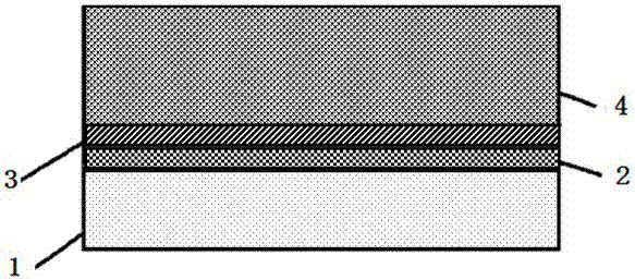
[0021] refer to figure 1 A method for growing a zinc oxide film using buffer layer technology of the present invention comprises the following steps: plating a nickel-zinc composite buffer layer on a 2-inch c(0006) plane sapphire substrate 1 by vacuum evaporation, and electron beam evaporation coating The rate is 0.1nm / s, the nickel buffer layer 2 is plated first, and then the zinc buffer layer 3 is plated, the thickness of each layer is 10nm, and the total thickness of the nickel-zinc composite buffer layer is 20nm. Then a zinc oxide thin film 4 is grown on the nickel-zinc composite buffer layer by pulsed laser deposition.

[0022] In the pulsed laser deposition method described in this embodiment, the background vacuum degree of the growth chamber is 6.3×10 -4 Pa, the light source is a KrF excimer laser with a wa...


PUM

PropertyMeasurementUnit
thicknessaaaaaaaaaa

Abstract

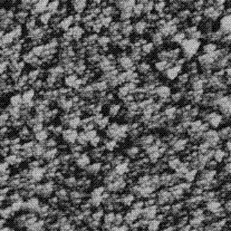
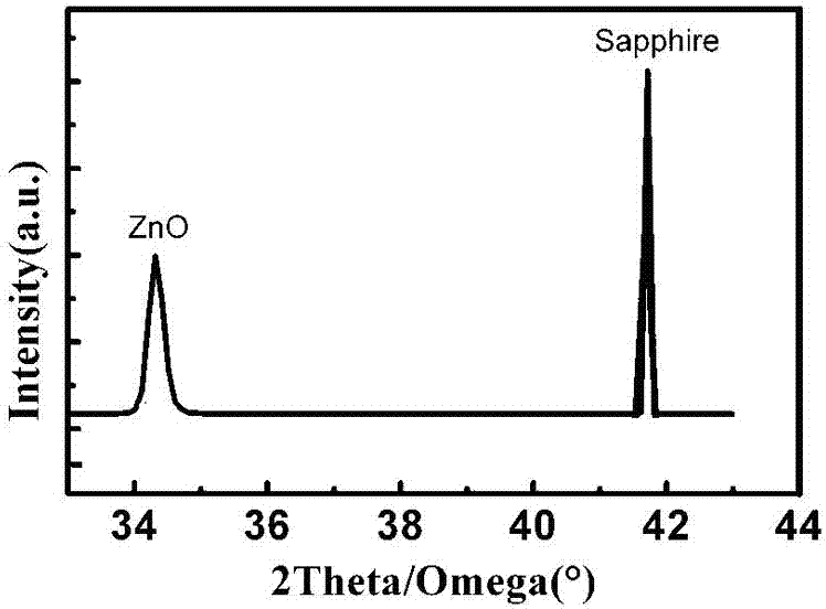
The invention discloses a method for growing a zinc oxide thin film by using buffer layer technology, which is characterized in that: a nickel-zinc composite buffer layer is plated on a sapphire substrate first, and then grown on the nickel-zinc composite buffer layer by a pulse laser deposition method Zinc oxide thin film; the method can effectively control the growth of ZnO thin film material, the method is simple and easy, the production efficiency of ZnO thin film material is improved, the process is simple, and the production cost is low. The surface of the prepared zinc oxide film is smooth, and the peak of the PL (photo-luminescence) test spectrum is clear, which meets the basic requirements of optoelectronic devices.

Description

technical field [0001] The invention relates to a method for growing a zinc oxide thin film using buffer layer technology, in particular to a method for growing a zinc oxide thin film on a nickel-zinc composite buffer layer using a pulsed laser deposition (PLD) method. Background technique [0002] Zinc oxide (ZnO) is a wide-bandgap (about 3.37eV at room temperature) II-VI compound semiconductor material with excellent optical and electrical properties. Especially in the rapid development in the past two decades, it has been widely used in transparent conductive films, surface acoustic wave devices, gas sensors and optoelectronic devices. Compared with the wide bandgap semiconductor material GaN, ZnO has many advantages. The growth temperature of ZnO thin film (also known as ZnO epitaxial wafer in industry) is generally lower than 700°C, which is lower than that of GaN (growth temperature about 1050°C); ZnO thin film has high energy conversion efficiency in photoluminescenc...

Claims


Application Information

Patent Timeline
Patent Type & Authority Patents(China)
IPC IPC(8): C23C14/28C23C14/08C23C14/30C23C14/18
Inventor 熊辉叶苍竹师岩峰官守军吕奎
Owner 黄石晨信光电股份有限公司
Learn More