

Gate-all-around anti-irradiation MOS field effect transistor based on 65 nm technology
A field effect tube and anti-irradiation technology, applied in transistors, electrical components, circuits, etc., can solve problems that threaten circuit and system reliability, drift of device threshold voltage, increase of off-state leakage current, etc., and achieve strong anti-total dose Irradiation capability, off-state leakage current reduction, effect of leakage current reduction
- Summary
- Abstract
- Description
- Claims
- Application Information
AI Technical Summary
Problems solved by technology
Method used
Image

Examples
example 1
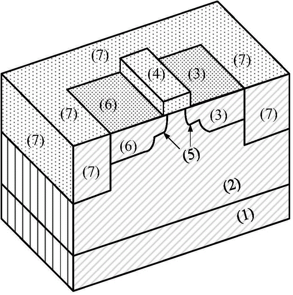
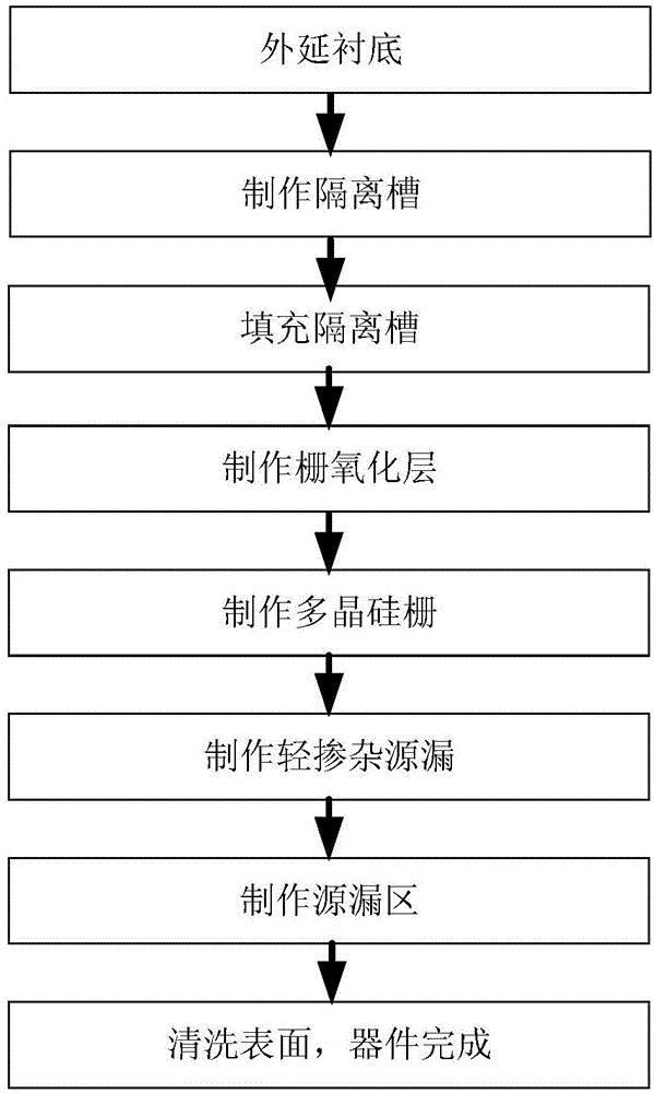
[0045] Example 1, making a 65nm MOS field effect transistor with a square gate ring.
[0046] Step 1, growing an epitaxial layer.
[0047] 1.1) Using the method of chemical vapor deposition at a temperature of 650 ° C with SiH 4 An epitaxial layer with a thickness of 1200nm is grown on a P-type substrate as a reactant;
[0048] 1.2) The depth of the epitaxial layer is 150nm, the concentration is 1×10 18 cm -3 doping to adjust the channel concentration.
[0049] Step 2, etching the isolation groove.
[0050] 2.1) Thin SiO with a thickness of 10nm is thermally oxidized on the epitaxial layer at a temperature of 1250°C by dry oxygen process 2 buffer layer, then the SiO 2 25nm thick Si grown on the buffer layer 3 N 4 The protective layer;
[0051] 2.2) In Si 3 N 4 A layer of photoresist is made on the protective layer, and the Si 3 N 4 Make a square ring-shaped isolation groove window on the photoresist around the protective layer and etch to form an isolation groove ...
example 2
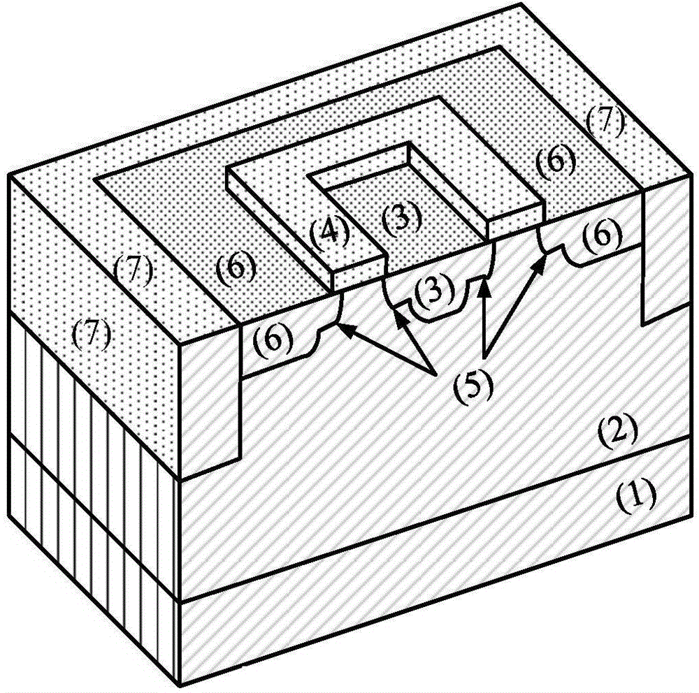
[0071] Example 2, manufacturing a 65nm MOS field effect transistor with a rectangular gate ring.
[0072] Step 1, using chemical vapor deposition method at a temperature of 600 ° C with SiH 4 An epitaxial layer with a thickness of 900nm was grown on a P-type substrate as a reactant, and then the depth of the epitaxial layer was 125nm, and the concentration was 7×10 17 cm -3 doping to adjust the channel concentration.
[0073] Step 2, etching the isolation groove.
[0074] Thin SiO with a thickness of 8 nm was grown by thermal oxidation at a temperature of 1200 °C on the epitaxial layer by a dry oxygen process 2 buffer layer, then the SiO 2 22nm thick Si grown on the buffer layer 3 N 4 protective layer; in Si 3 N 4 A layer of photoresist is made on the protective layer, and the Si 3 N 4 Make a rectangular ring-shaped isolation groove window on the photoresist around the protective layer and etch to form an isolation groove with a width of 400nm; after the etching is c...
example 3
[0086] Example 3, manufacturing a 65nm MOS field effect transistor with a circular gate ring.
[0087] Step A, growing an epitaxial layer.
[0088] A1) using chemical vapor deposition method at a temperature of 550 ° C with SiH 4 An epitaxial layer with a thickness of 600nm is grown on a P-type substrate as a reactant;
[0089] A2) The depth of the epitaxial layer is 100nm, the concentration is 2×10 17 cm -3 doping to adjust the channel concentration.
[0090] Step B, etching the isolation groove.
[0091] B1) Thin SiO with a thickness of 5 nm is thermally oxidized on the epitaxial layer at a temperature of 1100 ° C by a dry oxygen process 2 buffer layer, on SiO 2 20nm thick Si grown on the buffer layer 3 N 4 The protective layer;
[0092] B2) in Si 3 N 4 A layer of photoresist is made on the protective layer, and the Si 3 N 4 A circular ring-shaped isolation groove window is made on the photoresist around the protective layer and etched to form an isolation groov...
PUM
 Abstract
Description
Claims
Application Information